


Buyer Guides
HDI PCB design: Via Cost Comparison: Blind vs Buried vs Through Vias
May
The via itself is not the expensive part
Here’s the ugly truth: buyers often ask, “How much does a blind via cost?” as if the via were a screw, a connector, or a resistor on a BOM.
It isn’t.
A via is a process decision hiding inside the stack-up. That decision touches drilling, lamination, plating, registration, AOI, impedance control, scrap risk, and sometimes the whole order schedule. Cheap on paper. Dangerous in production.
I’ve seen a board look reasonable in Gerber review, then become painfully expensive after the stack-up was opened. Why? Not because the factory wanted to “charge more.” Because one buried via pair forced an extra lamination cycle, and one blind via layer pair turned a normal multilayer PCB into an HDI build with tighter registration requirements.
That’s the trap.
In HDI PCB via design, through vias are usually the lowest-cost path, blind vias are the density tool, and buried vias are the expensive internal-routing weapon that should be used only when they solve a real layout problem. Simple? Yes. But designers still ignore it.
Why?
Because CAD tools make every via look equally easy.
Through vias: cheap, familiar, and physically rude
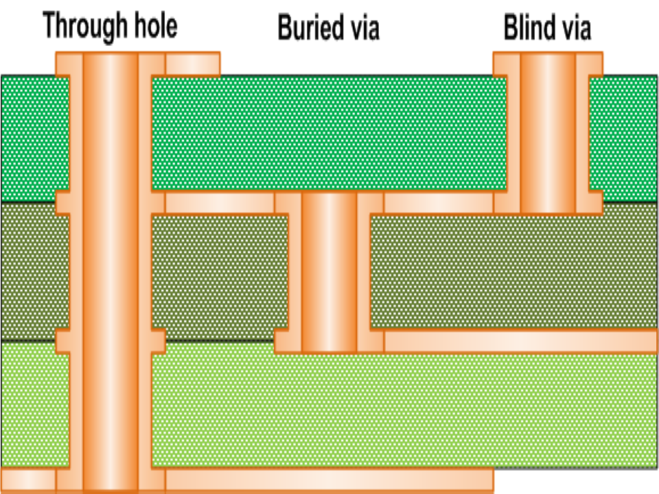
Through vias go from the top layer to the bottom layer. They are drilled after lamination, plated through, and inspected with processes every serious PCB shop already understands.
No magic there.
For standard multilayer boards, through-hole vias are the cost baseline because they do not require sequential lamination or laser-drilled microvia structures. The factory drills, plates, images, etches, finishes, tests, and ships. That’s why through vias are still everywhere: industrial controls, power boards, appliance controllers, basic communication modules, and plenty of medical support hardware that doesn’t need extreme component density.
But through vias are not polite guests. They pass through layers they may not electrically need, block routing channels, create stubs in high-speed nets, and can destroy fanout space under fine-pitch BGAs. In dense HDI work, that cheap hole becomes expensive because it eats layout area.
I frankly believe many engineers overuse HDI because they under-plan through-via placement. A 0.20 mm laser via sounds advanced. A cleaner fanout plan is often better.
For boards where cost matters more than maximum density, a conventional multilayer approach can still be the smart choice. If the product sits closer to industrial control, sensor interface, or appliance electronics, something like a high-frequency refrigerator control PCB panel may not need buried vias at all.
Blind vias: the density upgrade buyers actually understand
Blind vias connect an outer layer to one or more inner layers without passing through the full board. In HDI, the common version is a laser-drilled microvia from L1-L2 or L1-L3, often with copper filling when via-in-pad is needed.
Small hole. Big bill.
Why does cost rise? Laser drilling is only part of it. The real cost comes from registration control, copper plating consistency, resin behavior, lamination planning, and yield loss when the design pushes too close to process limits. A blind via is not just “shorter than a through via.” It changes how the board is built.
For smartphones, RF modules, compact medical devices, wearable electronics, high-pin-count BGA products, and dense communication boards, blind via PCB design is often justified. You win routing space. You reduce through-via congestion. You avoid unnecessary layer penetration. You can escape fine-pitch BGAs without turning the board into a routing disaster.
But don’t romanticize it.
A 1+N+1 HDI stack-up is manageable. A 2+N+2 stack-up starts asking more from lamination and alignment. Stacked microvias? Now we’re talking about plating reliability, copper fill, thermal stress, and supplier capability. If the buyer only says “make it cheaper” after choosing stacked blind vias, that’s not purchasing strategy. That’s denial.
For projects where the product really needs fine-pitch routing and compact mechanical size, a supplier experienced in B2B OEM multi-layer HDI PCB fabrication for fine pitch is a safer match than treating HDI like ordinary FR-4 purchasing.
Buried vias: useful, expensive, and often abused
Buried vias connect internal layers only. They do not reach the outside surfaces. That sounds elegant.
It is also costly.
A buried via usually means the inner layer subassembly must be drilled and plated before final lamination. That adds process steps. More process steps mean more chances for misregistration, plating issues, lamination shift, and scrap. This is why buried vias vs through vias is not a small price discussion; it is a manufacturing route discussion.
I’ll say the part many sales pages avoid: buried vias are often used because the first layout attempt was too ambitious for the chosen board size, not because the product truly needed them.
Sometimes they are justified. For dense RF routing, internal escape channels, EMI-sensitive layouts, or compact medical electronics, buried vias can clean up the layer structure. In complex communication boards, they may support signal integrity by keeping certain transitions internal and reducing surface congestion. That fits designs like a multilayer Rogers HDI PCB mainboard for communication PCB, where material choice, controlled impedance, RF behavior, and HDI routing all interact.
But if a buried via is only there because nobody wanted to add 2 mm to board length, pause.
That 2 mm may be cheaper than a second lamination cycle.
The real cost ladder: not theory, quoting desk reality
In 2024 quote reviews, the cost jump I most often saw did not come from “HDI” as a label. It came from stack-up escalation. A plain 6-layer board with through vias might stay comfortably inside a standard process window. Add blind microvias from L1-L2, and the quote moves. Add buried vias between L3-L4, and now the board may need sequential lamination. Add filled stacked microvias and fine-line trace/space, and the buyer suddenly asks why the prototype price feels like a small machine part.
That’s normal.
Here is a practical cost comparison. These are not universal prices; they are working ranges for buyer thinking when Gerbers are still adjustable.
| Via Type | Typical Structure | Cost Level | Main Cost Driver | Best Use Case | Common Mistake |
|---|---|---|---|---|---|
| Through via | Top to bottom | Low | Mechanical drilling and plating | Standard multilayer PCB, lower-density routing | Using too many under fine-pitch BGA areas |
| Blind via | Outer layer to inner layer | Medium to high | Laser drilling, registration, copper fill, HDI lamination planning | Fine-pitch BGA escape, compact HDI PCB via design | Adding blind vias everywhere instead of only where density requires |
| Buried via | Inner layer to inner layer | High | Extra drilling, plating, and sequential lamination | Internal routing channels, advanced RF or compact medical boards | Using buried vias to fix poor early stack-up planning |
| Stacked microvia | Microvias vertically stacked | Very high | Copper filling, plating reliability, thermal cycling risk | Ultra-dense BGA and miniaturized electronics | Choosing stacked vias before checking staggered alternatives |
| Staggered microvia | Microvias offset layer by layer | High but safer than stacked in many builds | HDI registration and routing discipline | Dense designs needing better reliability margin | Assuming staggered vias always route as tightly as stacked vias |
Blind vias vs buried vias: the buyer’s painful question
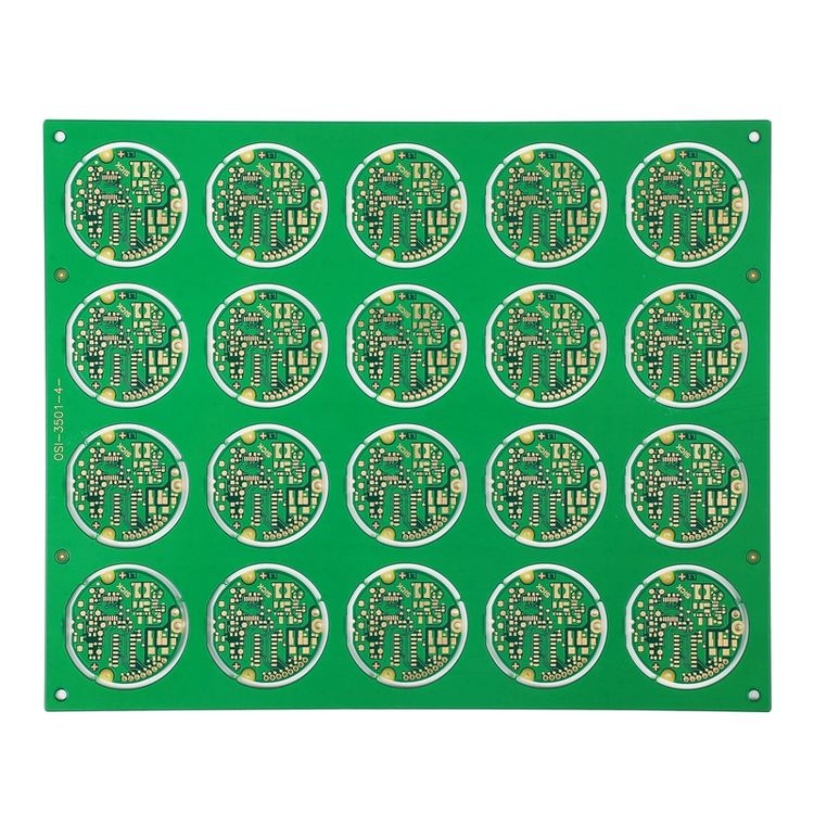
Blind vias usually give more visible routing value per dollar than buried vias because they help solve surface escape problems directly. Buried vias help internal routing, but they can add process complexity that is harder for buyers to see until the quotation arrives.
That’s the clean answer.
But the real answer depends on where the density problem lives. If the problem is BGA fanout from the top layer into inner signal layers, blind vias are the natural tool. If the problem is internal layer congestion after signals are already inside the board, buried vias may be justified. If neither problem exists, through vias probably win.
I know that sounds blunt.
Good.
HDI PCB microvia cost is often inflated by vague layout habits: oversized board fear, last-minute layer changes, uncontrolled via-in-pad usage, and stack-ups copied from a previous project that had different signal density. Copy-paste stack-up design is expensive laziness.
For rigid-flex products, the issue becomes even more sensitive because the via choice must respect bend zones, rigid area transitions, adhesive systems, and mechanical stress. In that case, early collaboration on OEM HDI rigid-flex PCB design with custom rigid-flex FPC can prevent the classic mistake: beautiful routing, ugly fabrication yield.
The 3 hidden cost bombs in HDI PCB via design
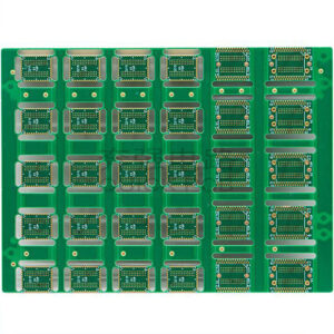
1. Sequential lamination
One lamination cycle is normal. Two is expensive. Three is painful.
Sequential lamination means the PCB is built in stages. Drill and plate part of the stack. Laminate again. Drill again. Plate again. Each round adds time, risk, and inspection burden. This is why buried vias can cost more than buyers expect. They may force an inner sub-build before the final board exists.
The cost is not just labor. It is yield math.
If each process stage has a small defect probability, adding more stages multiplies risk. A 95% yield process repeated through multiple sensitive steps does not magically remain 95%. It drops. And when the board uses high-frequency material, thin dielectrics, small annular rings, and tight impedance tolerances, the margin gets thinner.
2. Via filling and planarization
Via-in-pad looks clean on the layout. On the factory floor, it means copper filling or conductive/non-conductive filling, planarization, plating cap control, and surface flatness checks.
Not optional.
If a BGA pad sits on an open via, solder can wick into the hole. Assembly yield suffers. If the fill is poor, the pad can become uneven. If planarization is sloppy, solder joint quality pays the price. So when someone asks why blind via PCB design costs more with via-in-pad, I don’t need a long speech. The pad is no longer just a pad.
It is a small manufacturing contract.
3. Material and impedance interaction
HDI routing often appears in high-speed or RF products. That means via cost cannot be separated from dielectric thickness, Dk/Df values, copper roughness, impedance tolerance, and stack-up symmetry.
For high-frequency designs, the via transition may affect signal behavior. For medical or communication electronics, stable performance matters more than shaving a few cents. That is why a project needing HDI high-frequency PCB assembly one-stop OEM B2B service should be discussed as a full build strategy, not a hole-price negotiation.
How I would choose: blind, buried, or through?
Use through vias first unless density, signal integrity, or mechanical constraints prove they are not enough.
That is my bias.
Then add blind vias only where they solve a clear routing bottleneck, usually under fine-pitch packages or dense surface routing zones. Keep the blind via structure simple if possible: L1-L2, L1-L3, or 1+N+1 before jumping into stacked complexity.
Buried vias come later. Not never. Later.
They make sense when internal routing density is genuinely blocked and adding layers would be worse than adding buried interconnects. They also make sense in some compact high-reliability devices, including miniaturized medical electronics, where board area is fixed and signals cannot simply spread out. For that category, OEM medical HDI PCB supplier support for high-reliability devices matters because the cost conversation must include test strategy, traceability, and build consistency.
Cost control checklist before sending Gerbers
Before asking for a final price, I would check these points:
| Design Question | Why It Changes Cost | Better Buyer Action |
|---|---|---|
| Can some blind vias become through vias outside BGA zones? | Reduces laser drilling and HDI process load | Separate dense and non-dense routing areas |
| Is the buried via solving a real internal congestion issue? | Buried vias may force sequential lamination | Ask for a no-buried-via stack-up alternative |
| Are stacked microvias truly needed? | Stacked structures raise plating and reliability demands | Compare staggered microvias first |
| Is via-in-pad used only where necessary? | Filling and planarization add cost | Limit it to fine-pitch packages |
| Can board size grow slightly? | Extra area may be cheaper than advanced vias | Compare cost of +5% board area vs HDI escalation |
| Is impedance tied to the via plan? | Via transitions affect high-speed behavior | Review stack-up, material, and via geometry together |
| Is the prototype stack-up the same as mass production? | Prototype shortcuts may fail at volume | Quote both prototype and production routes early |
The controversial part: cheaper HDI is often decided before quotation
Most buyers negotiate too late.
Once Gerbers are finished, the supplier can only price the pain already designed into the board. The real savings happen earlier: package selection, BGA pitch choice, board outline, stack-up planning, via structure, routing rules, and whether the designer was allowed to add one more layer before creating a buried-via monster.
I have seen an 8-layer design with careful blind vias beat a 10-layer board with lazy through-via congestion. I have also seen a slightly larger 6-layer board beat an over-tight 8-layer HDI board on both cost and delivery.
Tiny boards are not always cheaper.
In HDI PCB via design, the cheapest board is not the board with the fewest layers. It is the board with the cleanest manufacturing path.
FAQ
What is the cheapest via type in HDI PCB via design?
The cheapest via type in HDI PCB via design is usually the through via because it uses standard mechanical drilling and plating after lamination, without the extra laser drilling, copper filling, or sequential lamination often required by blind and buried via structures in dense multilayer boards. Through vias remain the practical baseline for cost comparison.
That does not mean through vias are always the best choice. If they block BGA escape routing or create long stubs in high-speed nets, the layout may need more layers, more board area, or later redesign. Cheap can become expensive when it steals routing space.
Are blind vias more expensive than through vias?
Blind vias are more expensive than through vias because they usually require laser drilling, tighter layer registration, controlled plating, and sometimes copper filling when used as via-in-pad under fine-pitch components such as 0.4 mm or 0.5 mm pitch BGAs. They cost more because the fabrication route becomes more demanding.
Still, blind vias can save total product cost when they reduce layer count or allow a compact board outline. A blind via used under a dense BGA may be cheaper than expanding the PCB size, adding layers, or forcing a painful reroute.
Why do buried vias cost more than blind vias?
Buried vias often cost more than blind vias because they are formed inside the PCB stack before final lamination, which can require drilling, plating, inspection, and lamination in separate stages before the full board is completed. That extra process route increases production time, alignment risk, and scrap exposure.
The painful part is that buried vias are invisible in the finished board, so buyers may not understand why they cost so much. The factory sees the extra build sequence. The quote reflects that sequence.
Should I use blind vias or buried vias for fine-pitch BGA fanout?
Blind vias are usually the better first choice for fine-pitch BGA fanout because they help escape signals from the outer component layer into nearby internal routing layers without consuming the entire board thickness like through vias. Buried vias should be considered later if internal routing congestion still blocks the design.
For many 0.4 mm and 0.5 mm pitch BGA layouts, blind microvias from L1-L2 or L1-L3 are the normal starting point. Buried vias may help, but they should not be the first answer unless the stack-up analysis proves they are needed.
How can I reduce HDI PCB microvia cost?
You can reduce HDI PCB microvia cost by limiting blind vias to dense routing zones, avoiding unnecessary stacked microvias, checking staggered structures first, reducing via-in-pad usage, and asking your PCB supplier to compare at least two stack-up options before final Gerber release. Cost control starts before quotation.
The best move is simple: ask for DFM feedback while the layout is still flexible. Once the design is frozen, every cost-saving idea becomes harder, slower, and more political.
When are buried vias worth the extra cost?
Buried vias are worth the extra cost when they solve internal routing congestion that cannot be fixed by better fanout, slightly larger board size, cleaner layer assignment, or a simpler blind-via structure. They are most defensible in compact HDI, RF, medical, and advanced communication boards where routing density is genuinely locked.
My rule is harsh but useful: if removing the buried via does not break routing, signal performance, or mechanical size limits, remove it. Buried vias should earn their place.
Conclusion
If your HDI quote looks too high, do not start by squeezing the supplier. Start by checking the via structure.
Send the stack-up, Gerbers, drill files, impedance needs, material requirement, finish, copper weight, and target quantity. We can review whether your board really needs blind vias, buried vias, stacked microvias, or a cleaner through-via route — and we can suggest a more manufacturable path before the cost gets locked into the design.
