













Tag Archives: HDI PCB design

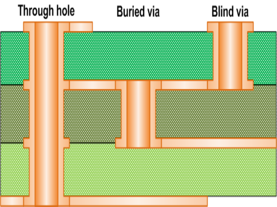
HDI PCB design: Via Cost Comparison: Blind vs Buried vs Through Vias

Via Cost Comparison: Blind vs Buried vs Through Vias

Blind, buried, and through vias do not cost the same because they do not stress the factory in the same way. This guide explains where via cost really comes from in HDI PCB via design, and how buyers can cut cost without damaging reliability.
HDI PCB Design: Requirements, Benefits, and Complexities

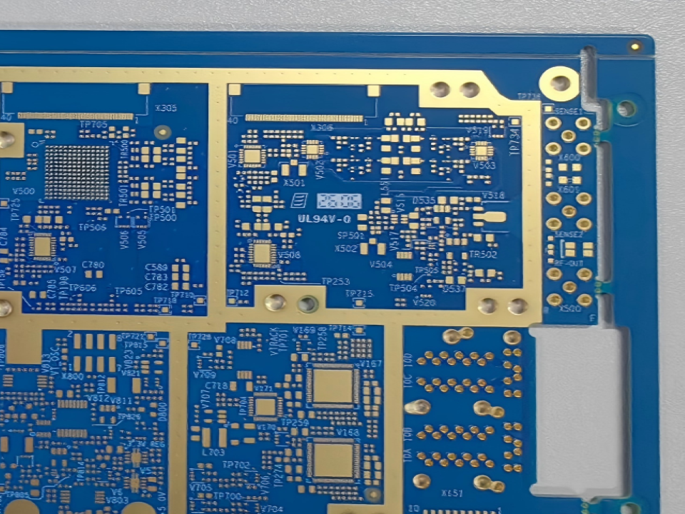
HDI PCB Design: Requirements, Benefits, and Complexities

HDI PCB design isn’t just about shrinking a board; it’s about controlling vias, stackup, materials, yield, and cost before layout becomes a factory problem. This article explains the real requirements, benefits, and complexities behind high density interconnect PCB design.