


Buyer Guides
HDI PCB Design: Requirements, Benefits, and Complexities
May
I’ve seen HDI used beautifully. I’ve also seen it used like expensive makeup on a bad layout.
Big difference.
A clean HDI PCB can make a product smaller, faster, lighter, and easier to package, but when the stackup is chosen too late, when microvias are thrown in just to rescue routing, or when nobody checks the fabricator’s real laser-drill and copper-fill limits, the board doesn’t become “advanced.” It becomes a quiet production headache.
And yes, the headache usually appears after the prototype looks fine.
What HDI PCB Design Really Means
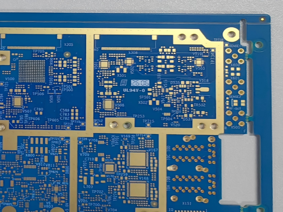
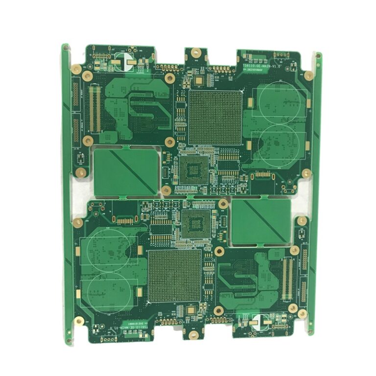
HDI PCB design means using high density interconnect structures—microvias, blind vias, buried vias, fine traces, tight spacing, via-in-pad, and build-up stackups—to route more signals in less space.
That’s the clean definition. The shop-floor definition is uglier: HDI is what you need when through-holes waste too much routing room and the BGA pitch starts bullying the layout.
For fine-pitch electronics, especially where the board size is already fixed, HDI isn’t a luxury option. It’s often the only sane routing method left. You can see this kind of manufacturing direction in B2B OEM multi-layer HDI PCB fabrication for fine-pitch applications.
But I frankly believe many teams choose HDI too late. They finish placement, get trapped by escape routing, panic, and then ask the PCB factory to “make it work.”
That’s backwards.
Don’t Start With Layer Count
“Should we use 8 layers or 10 layers?”
Bad first question.
The better question is: what’s the tightest package on the board, what’s the escape route, how many signal layers need clean return paths, and what microvia structure can actually be built repeatedly without turning yield into a casino?
Layer count is not strategy. It’s the bill you receive after strategy fails—or succeeds.
| Requirement Area | What It Means | Why It Matters |
|---|---|---|
| Minimum trace and space | Often 3/3 mil, 2.5/2.5 mil, or tighter depending on factory capability | Push it too far and yield starts bleeding |
| Microvia diameter | Laser-drilled vias between selected layers | Saves space, but plating quality becomes sensitive |
| HDI PCB stackup | 1+N+1, 2+N+2, or advanced build-up | Controls lamination cycles, routing freedom, and cost |
| Via structure | Staggered, stacked, blind, buried, or via-in-pad | Affects reliability more than buyers think |
| Material choice | FR-4, high-Tg FR-4, low-loss laminate, hybrid stackup | Impedance, thermal expansion, and drilling all depend on it |
| Copper plating | Especially inside filled microvias | Weak plating can pass sample test and fail later |
| DFM review | Factory manufacturability check before release | Saves redesign time and awkward emails |
Here’s the ugly truth: passing CAD DRC doesn’t mean the board is manufacturable.
It means the software didn’t complain.
Stackup Is Where the Money Hides
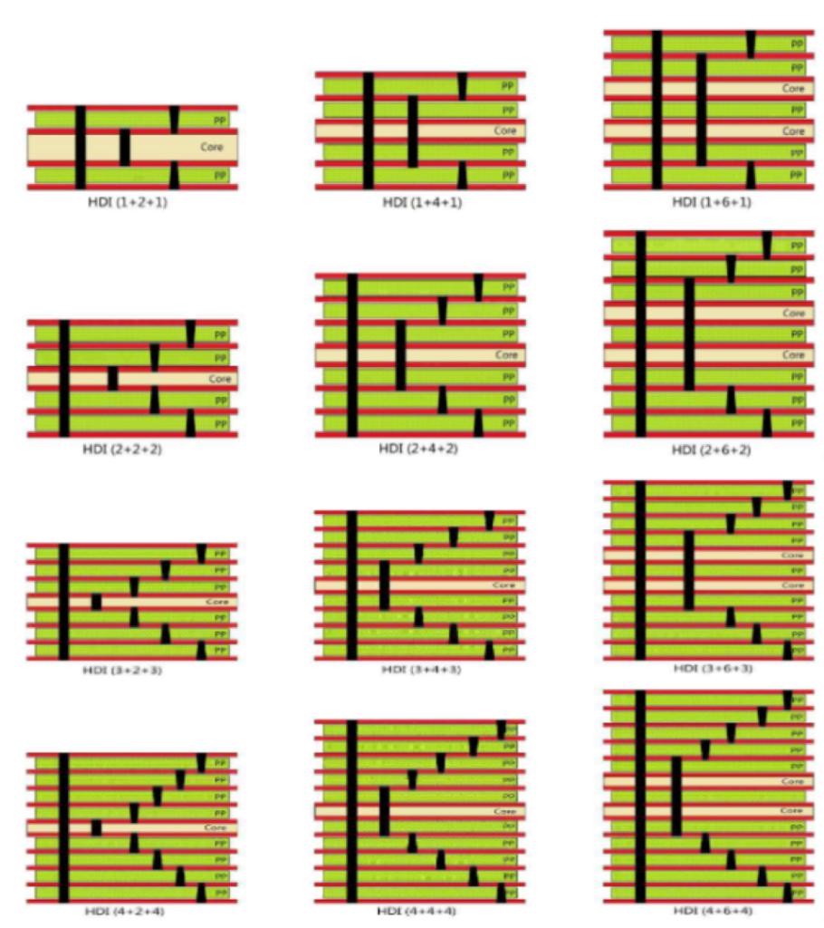
HDI PCB stackup looks like a technical drawing. It’s actually a financial decision.
A 1+N+1 stackup means one build-up layer on each side of the core. A 2+N+2 stackup means two build-up layers on each side. More build-up means more lamination, more laser drilling, more filling, more plating, more registration risk, and more inspection.
More pain, basically.
For example, a 1+6+1 HDI board may be enough for many compact products. A 2+4+2 structure gives more escape freedom under fine-pitch BGAs, but the cost jump can be sharp. Stacked microvias can save space, sure, but they’re less forgiving than staggered vias. Via-in-pad can be excellent, but only when filling and planarization are properly defined.
If the product doesn’t truly need HDI, don’t force it. For many control boards, OEM FR4 multilayer PCB manufacturing for control boards is still the more stable and cheaper route.
Boring wins. Often.
Microvia PCB Design: Tiny Hole, Expensive Lesson
Microvias are small. Their problems are not.
From my experience, microvia decisions are where a lot of HDI designs quietly become risky. Not during the first power-on test. Not when the sample photos look beautiful. Later—after reflow, thermal cycling, vibration, or field use.
A microvia is not just a dot in the layout. It’s a plated mechanical structure, and it has to survive stress.
Watch these details:
- Aspect ratio
- Laser drill quality
- Copper plating uniformity
- Via filling quality
- Stacked versus staggered structure
- Dielectric thickness
- Reflow exposure
- Application temperature range
For consumer electronics, some risk may be acceptable. For aerospace, medical, automotive, and industrial equipment, the same via decision becomes a reliability argument.
This is why I don’t love “just stack the vias” as a casual answer. Sometimes stacked vias are needed. Sometimes they’re just a lazy escape hatch with a nice-looking layout screenshot.
Blind and Buried Vias: Useful, But Not Free
Blind and buried vias HDI PCB structures help route dense boards by connecting only the layers that need to connect.
Simple idea.
Blind vias connect an outer layer to an inner layer. Buried vias connect inner layers without reaching the surface. Microvias often act as blind vias in HDI designs. This gives more routing channels, cleaner BGA escape, and better use of internal layers.
But nobody should pretend they’re free.
Blind and buried vias add process steps. They can require sequential lamination. They make inspection harder. They increase scrap exposure because defects may already be buried before the board is complete.
My bias? Use blind and buried vias when the routing proves they’re needed—not because the design wants to look “high-end.”
HDI PCB Benefits, Without the Sales Perfume
HDI PCB benefits are real: smaller board size, higher wiring density, better fine-pitch BGA breakout, shorter interconnects, lower parasitics, and more layout freedom.
That’s the brochure version.
The real version is this: HDI lets product teams keep adding functions while pretending the enclosure size didn’t change. More sensors. More wireless. More memory. More power control. More shielding. More connectors crammed into the same mechanical box.
It helps. It doesn’t perform magic.
For smart displays or compact industrial panels, a standard multilayer board may still work. If the product sits between normal FR-4 and HDI density, review B2B FR-4 control PCB manufacturing for smart display panels before jumping straight into a costly HDI stackup.
Where HDI PCB Complexity Usually Hides
The schematic won’t warn you.
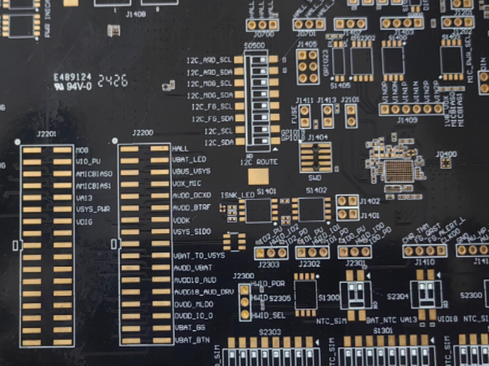
HDI PCB complexity hides in fab notes, tolerances, drill tables, copper specs, resin behavior, impedance coupons, filled-via requirements, and the difference between “we can prototype it” and “we can build 5,000 pieces without drama.”
| Complexity Point | Common Mistake | Better Approach |
|---|---|---|
| Fine trace routing | Designing below stable factory capability | Match trace/space to real production limits |
| Via-in-pad | Forgetting filled and capped via requirements | Define filling, plating, and planarization clearly |
| Stacked microvias | Using them casually to save space | Prefer staggered vias where possible |
| Impedance control | Treating HDI only as density work | Build stackup around signal behavior early |
| Material choice | Using standard FR-4 for everything | Consider high-Tg or low-loss material when needed |
| Cost planning | Asking price after layout is frozen | Discuss via structure before final routing |
| Testing | Relying only on basic E-test | Add AOI, X-ray, microsection, or impedance testing when risk is high |
Looks clean. Isn’t simple.
That’s HDI.
How to Design an HDI PCB Without Trapping Yourself
How to design an HDI PCB properly? Start with the densest component, map the escape routing, choose the simplest stackup that works, control microvia structure, confirm factory limits, and run DFM before the layout becomes politically impossible to change.
Yes, politically. Anyone who has worked with late-stage hardware changes knows what I mean.
A practical HDI process looks like this:
- Find the tightest BGA, module, or connector.
- Decide escape routing before final placement.
- Choose whether microvias are truly needed.
- Pick 1+N+1, 2+N+2, or another build-up structure.
- Avoid stacked microvias unless space leaves no better option.
- Confirm trace, space, annular ring, copper weight, and dielectric thickness with the factory.
- Lock impedance stackup before high-speed routing.
- Review DFM before Gerber release.
- Add testing based on product risk.
- Recheck cost before prototype habits become mass-production habits.
The most expensive sentence in PCB work is still: “The layout is already finished.”
I hate that sentence.
HDI Versus Standard Multilayer PCB
Standard multilayer PCB still wins plenty of jobs. I’ll say that directly.
If there’s no fine-pitch BGA, no extreme space pressure, no high-speed density issue, and no routing choke point, HDI may be overkill. Expensive overkill.
| Design Factor | Standard Multilayer PCB | HDI PCB Design |
|---|---|---|
| Routing density | Moderate | High |
| Typical via style | Through-hole vias | Microvias, blind vias, buried vias |
| Cost | Lower | Higher |
| Lead time | Shorter | Longer |
| BGA support | Limited for fine pitch | Better for fine-pitch packages |
| Manufacturing risk | Easier to control | More process-sensitive |
| Best use case | Control boards, power boards, general electronics | Compact, fine-pitch, high-density, high-speed products |
Sometimes the right answer isn’t HDI. Sometimes it’s mechanical. If the product needs folding, movement, or tight 3D packaging, rigid-flex PCB manufacturing for foldable flex circuits may solve the real problem better than forcing everything into one rigid HDI board.
Materials Are Not a Footnote
Buyers love asking for price first.
I get it. Everyone has pressure.
But with HDI, material choice changes everything: laser drilling, resin smear, copper adhesion, CTE behavior, impedance stability, CAF risk, thermal stress, and insertion loss. A consumer HDI board may run fine on high-Tg FR-4. A fast communication board may need lower-loss material. A lighting or power product may not need HDI at all; it may need thermal handling through OEM aluminum MCPCB panels for automotive LED lighting.
Different problem. Different board.
That’s the part people skip.
Why Cheap HDI Quotes Make Me Nervous
Here’s the ugly truth: HDI is expensive because it concentrates risk.
Laser drilling has to be controlled. Imaging has to be tighter. Lamination has more steps. Copper filling has to behave. Registration tolerance gets narrow. Inspection takes more work. Scrap costs more because the board has already absorbed more process time before the failure appears.
So when a supplier quotes suspiciously low without asking about stackup, microvia type, filled vias, impedance, laminate, copper thickness, and test requirements, I don’t feel happy.
I feel suspicious.
Maybe they understood it perfectly. Maybe. But usually, the missing questions show up later as missing quality.
When HDI PCB Design Makes Sense
HDI PCB design makes sense when the board needs high routing density, fine-pitch component escape, smaller size, shorter interconnect paths, cleaner signal routing, or more compact packaging than ordinary multilayer PCB can support.
Common use cases include:
- Wearables
- Medical handheld devices
- Aerospace modules
- Industrial compact controllers
- Automotive electronics
- Camera and sensor boards
- Communication modules
- Miniaturized IoT products
For general PCB and PCBA capability review, start from the PCB and PCBA product manufacturing overview and then decide whether the product needs HDI, standard FR-4 multilayer, aluminum MCPCB, flex PCB, or rigid-flex.
Not every design needs the same hammer.
The Best HDI Designs Are Usually Boring
I’ll be blunt: the best HDI PCB design is not the most aggressive one.
It’s the one that solves the density problem with the least risky structure.
Not the most layers. Not the smallest trace width. Not the flashiest stacked microvia chain. The best HDI board uses complexity only where the product forces it. Everywhere else, it stays boring, stable, and manufacturable.
That’s how prototypes become repeat orders.
FAQs
What is HDI PCB design?
HDI PCB design is the process of designing a high density interconnect printed circuit board with microvias, blind vias, buried vias, fine traces, compact stackups, and dense component placement to route more electrical connections in less physical space than a conventional PCB can usually support.
In plain language, HDI is used when normal through-hole routing wastes too much room. It’s common in fine-pitch BGA products, compact modules, wearables, medical devices, communication boards, and other electronics where size and routing density are both under pressure.
What are the main HDI PCB design requirements?
The main HDI PCB design requirements include controlled trace and space, reliable microvia structure, suitable laminate material, stable stackup design, correct via filling, impedance planning, copper plating control, and early DFM review with the PCB manufacturer before the layout is released for fabrication.
The dangerous part is not one single requirement. It’s the combination. Fine traces plus tight spacing plus stacked vias plus sequential lamination can work, but only when the factory capability matches the design ambition.
What are the benefits of HDI PCB design?
HDI PCB design benefits include smaller board size, higher wiring density, better fine-pitch BGA breakout, shorter signal paths, lower parasitic effects, improved routing freedom, and stronger support for compact electronic products with dense components and limited mechanical space.
But HDI is not automatically better. If a standard multilayer board can meet the product goal, HDI may only add cost, longer lead time, and more process risk.
Why is HDI PCB complexity higher than normal PCB design?
HDI PCB complexity is higher because it depends on laser-drilled microvias, tighter trace and space rules, sequential lamination, controlled copper filling, precise registration, impedance planning, and more detailed inspection than standard multilayer PCB fabrication normally requires.
The board may look simple after production. The process behind it is not simple at all.
How do microvias affect HDI PCB reliability?
Microvias affect HDI PCB reliability because they are small plated interconnects exposed to lamination stress, reflow heat, thermal cycling, mechanical strain, and long-term field conditions, so poor design or weak plating can create hidden failures after the prototype stage.
This is why stacked microvias deserve caution. Staggered structures are often more forgiving when the layout has enough space.
When should I choose HDI instead of standard multilayer PCB?
You should choose HDI instead of standard multilayer PCB when the product needs fine-pitch component escape, smaller board size, higher routing density, shorter interconnect paths, or more compact packaging than ordinary through-hole via routing can provide.
If standard multilayer routing works, use it. If it doesn’t, HDI becomes a serious engineering option—not just a prettier board type.
Conclusion
Don’t send an HDI project to quotation with only hope and Gerbers.
Send the stackup idea, BOM, Gerber files, target quantity, impedance needs, and application environment. We can help review whether the design truly needs HDI, which microvia structure is safer, and how to reduce cost before the layout becomes painful to change.
