















04
Jul
Jul
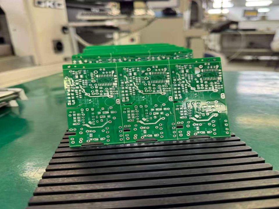
BGA heat does not disappear because the schematic passed review. This guide explains how PCB heatsink interface design, thermal vias, copper spreading, and TIM choices decide whether a BGA package survives real operating conditions.

Expert analysis of PCB industry innovations, emerging technologies, and market shifts from a leading Chinese manufacturer. Stay ahead with insights on HDI, flexible circuits, and advanced materials for global electronics markets.
BGA heat does not disappear because the schematic passed review. This guide explains how PCB heatsink interface design, thermal vias, copper spreading, and TIM choices decide whether a BGA package survives real operating conditions.
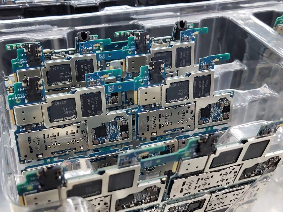
This post explains what turnkey, partial turnkey, consigned, and kitted PCB assembly really include. It helps buyers avoid BOM confusion, sourcing delays, and vague supplier responsibility before production starts.
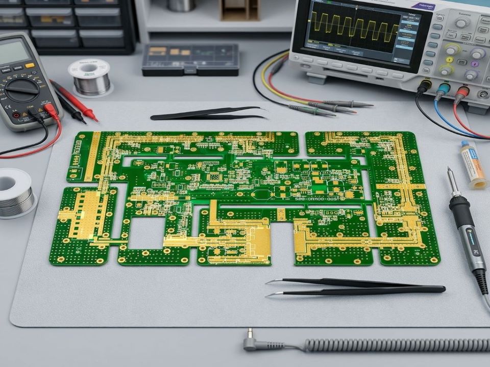
Prototype assembly is not just a production choice; it is a risk-management decision. This article breaks down the hard trade-offs between in-house PCB assembly and outsourced PCB assembly for engineering teams, buyers, and founders.

Setup fees can make a small PCB order look expensive, but per-unit cost can fall fast when batch size is planned correctly. This article explains how buyers should read batch production cost, avoid fake savings, and choose a smarter ordering quantity.
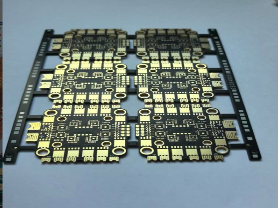
Mixed stackup design is not just a cheaper way to build a multilayer PCB. It is a controlled compromise between thermal stress, laminate behavior, reflow survival, and production yield.

Automotive PCBs don’t fail because someone forgot the phrase “High Tg.” They failed because they treated heat, copper, vias, resin, moisture, and reflow stress as separate issues.
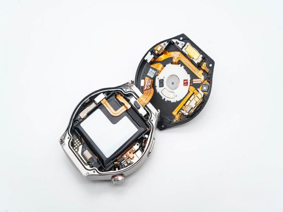
High-speed PCB design is not just faster routing; it is the discipline of keeping real electrical signals clean under imperfect materials, copper, vias, and manufacturing limits. This guide explains signal integrity fundamentals with practical layout judgment, fabrication reality, and the hard mistakes engineers usually learn too late.
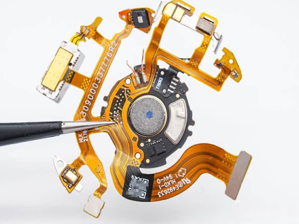
This article explains how HDI PCB design rules decide minimum via size, spacing, stack-up risk, and real manufacturability. It gives practical values, hard warnings, and a table engineers can use before sending Gerber files.
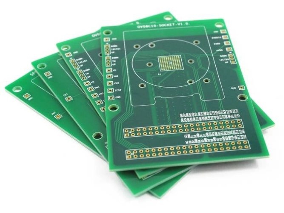
50-ohm impedance is not a magic trace width; it is a result of copper width, dielectric height, Dk, copper thickness, solder mask, and reference planes. This guide explains how PCB trace impedance calculation works before your RF or high-speed design reaches fabrication.
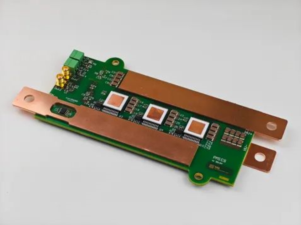
Rogers PCB prototyping gets expensive when material, impedance, and lead time collide. This article explains where the money really goes, why quick-turn RF boards aren’t simple, and how buyers can avoid bad prototype quotes.
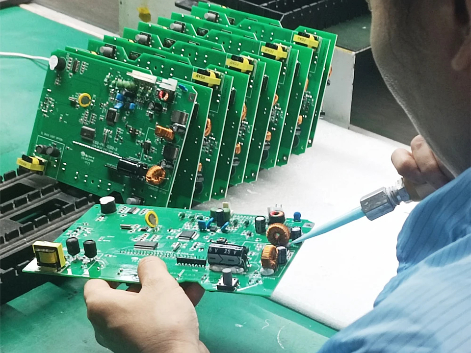
PCB pricing does not fall smoothly as order quantity rises; it breaks in actions when configuration, panel use, buying utilize, and yield threat adjustment. This article explains how quantity influences PCB manufacturing cost, where buyers pay too much, and what manufacturing facilities hardly ever say simply.
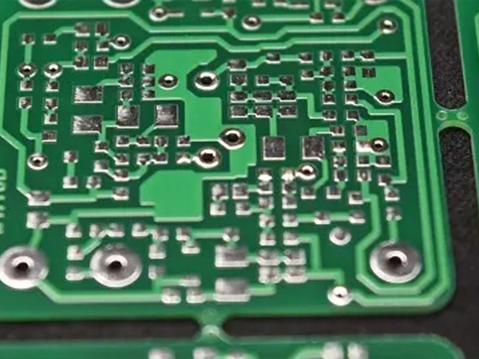
Global chip shortages don’t just slow PCB—they shift timelines into sourcing, alternates, ECOs, and re-test. Learn how to keep builds on track.