













Market Trends
BGA Thermal Connection: PCB Heatsink Interface Design
Jul
I’ve seen this mistake too many times: the BGA passes layout review, the first prototype powers up, everyone relaxes, and then two weeks later the unit starts acting weird in the chamber because the heat path was basically “some copper, some vias, and hope.”
That’s not design.
That’s gambling.
Here’s the ugly truth: most BGA overheating issues aren’t really heatsink problems. They’re interface problems. The heatsink gets blamed because it’s visible. The real mess is usually buried under the package — via structure, copper continuity, plane spreading, TIM thickness, solder voiding, enclosure tolerance, and sometimes one tiny mechanical gap that nobody priced into the project.
And the pressure is getting worse. According to the IEA, global data-center electricity consumption could reach around 945 TWh by 2030, with data-center demand growing about 15% per year from 2024 to 2030 . The DOE-backed Lawrence Berkeley National Laboratory report estimated U.S. data centers used about 176 TWh in 2023 and could reach 325–580 TWh by 2028.
More watts. Smaller boxes. Less mercy.
So when someone says, “Can we just add a heatsink later?” I get nervous.
BGA Heat Doesn’t Follow Your Nice Diagram
A BGA package doesn’t care how clean the schematic looks.
Heat can move up through the package lid into a heatsink. It can move down through solder balls into PCB copper. It can spread sideways through the substrate, copper planes, chassis metal, mounting screws, shielding cans, and sometimes even nearby connectors if the mechanical stack accidentally gives heat a better path.
Messy? Yes.
Real? Also yes.
For an FPGA, ASIC, AI accelerator, RF chip, processor, telecom module, or medical imaging controller, the thermal path usually looks like this:
Chip junction → package substrate → solder balls → PCB pads → thermal vias → internal copper planes → backside copper or chassis pad → TIM → heatsink or enclosure
Break one section and the whole chain gets worse. Not slightly worse. Sometimes dramatically worse.
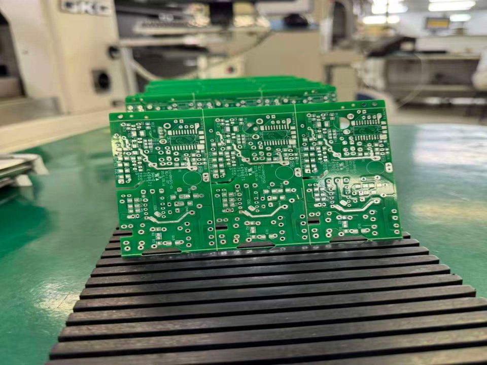
This is why I frankly believe BGA thermal management should be reviewed before routing gets too far. When the board is already packed with DDR, impedance lines, fanout vias, power islands, and keep-outs, thermal repair becomes expensive and ugly. For dense FPGA or control designs, early planning with a manufacturable structure like a custom PCB prototype for GPS, FPGA, and LCD control projects makes more sense than trying to “save” the layout at the end.
The Board Is Part of the Heatsink
People forget this.
A PCB isn’t only a carrier for signals; under a hot BGA, it becomes part of the thermal resistance stack, and that means layer count, dielectric thickness, copper weight, via fill, plane shape, solder mask opening, ENIG flatness, and copper balance all matter in ways that don’t show up in a normal BOM review.
Tiny detail. Big failure.
Texas Instruments’ PowerPAD layout guidance recommends thermal vias in the thermal pad area to move heat from top copper into inner or bottom copper layers. JEDEC thermal standards discussions also show why package thermal numbers need context, because test boards and real products are not the same animal.
That last part matters.
A datasheet θJA number isn’t your enclosure. θJC doesn’t magically mean your heatsink contact is good. ψJB isn’t a direct resistance value you can casually throw into a spreadsheet. And if the package vendor tested on a JEDEC board with controlled airflow, while your product sits in a sealed plastic case behind a warm display, congratulations — your “thermal model” is fiction.
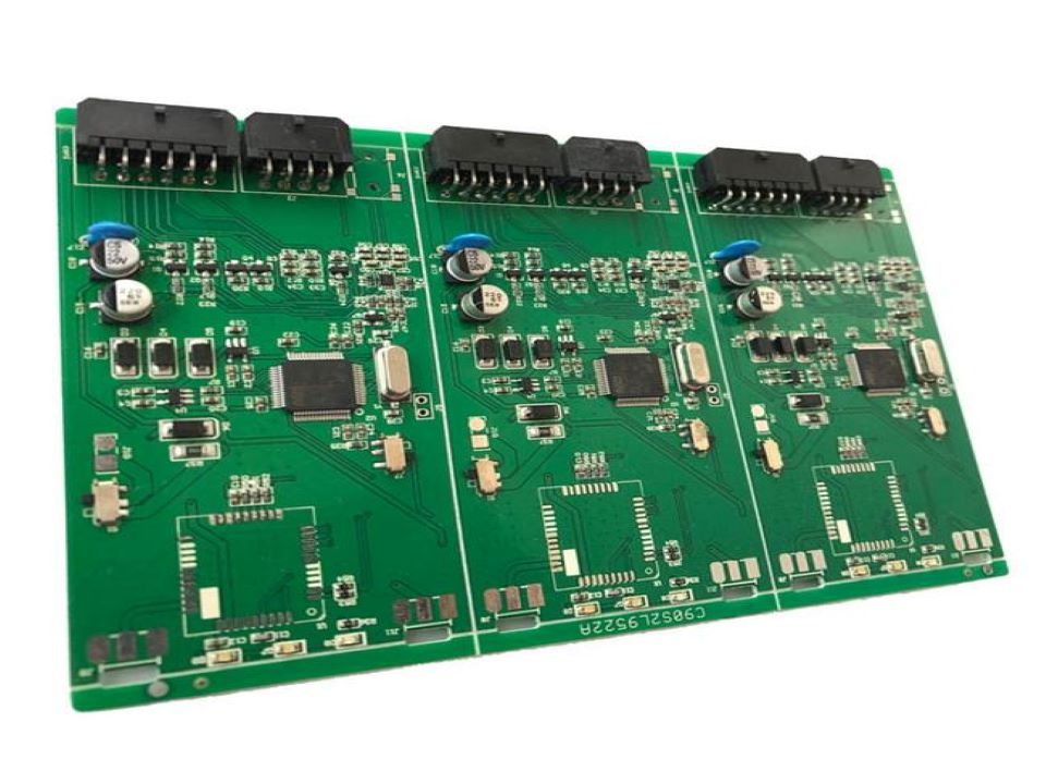
For fine-pitch BGA, HDI planning often becomes part of the thermal answer too. Via-in-pad, microvias, buried vias, filled/capped structures, and surface flatness all affect both routing and heat transfer. A process like an immersion gold HDI multilayer PCB panel fits this kind of work because pad reliability, coplanarity, ENIG solderability, and tight BGA geometry need to be controlled together.
Not separately.
Together.
Thermal Vias: Useful, Overused, and Often Misunderstood
Thermal vias are not decoration.
I know that sounds basic, but open enough PCB files and you’ll see the same habit: someone drops a grid of vias under the BGA, maybe connects a few to a plane, maybe forgets the copper destination entirely, and then everyone calls it BGA heat dissipation PCB design.
No.
A via only helps when it connects heat to somewhere useful. Large copper. A backside pad. A chassis contact. A metal stiffener. A real thermal spreading area.
If it ends in a skinny copper pour trapped between signal keep-outs, it’s just a plated hole with self-esteem.
The manufacturing side is just as annoying. Open vias near BGA pads can wick solder. Via-in-pad without proper filling and capping can starve joints. Poor cap plating can create planarity issues. Too much via density can fight routing and solder mask registration. And if nobody defines X-ray acceptance criteria, you’ll argue about voids after assembly instead of preventing them before production.
Fun? Not really.
A 2024 study on embedded minichannel heatsink structures in PCB assemblies showed how far engineers are pushing cooling closer to the board itself, especially when space and cost limit traditional cooling methods. I don’t think every BGA board needs embedded cooling channels. That would be ridiculous. But the direction is clear: heat removal is moving closer to the silicon and closer to the PCB stack.
For power or LED assemblies, the logic is even more obvious. A double-sided aluminum LED PCB panel works because it shortens the thermal route into metal. FR-4 can survive many applications, sure, but it’s not a hero material for heat.
Copper does the job. Metal does the job.
FR-4 mostly stands there.
TIM Is Where Good Designs Get Embarrassed
Thermal interface material looks simple on paper.
A pad says 3 W/m·K, 6 W/m·K, 12 W/m·K. A paste claims low bond-line thickness. A gap filler promises soft compression. The buyer compares unit price. The engineer checks the datasheet. Everyone thinks the decision is made.
It isn’t.
From my experience, TIM failures are often mechanical failures wearing a material disguise. The real questions are uglier: Is the pressure enough? Is the surface flat? Does the BGA lid sit lower than the nearby inductor? Does the heatsink rock on one screw boss? Is the gap pad too thick? Will the material pump out after thermal cycling? Is there air trapped because the dispense path was lazy?
That’s the shop-floor version.
A 2024 paper on thermal interface material dispense path planning noted that power electronics and ECUs face higher power densities and limited assembly space, and that engineers often rely on simulations plus manual trial-and-error before optimized dispensing improves coverage.
Translation: even the paste pattern can betray you.
A “better” TIM with poor contact can lose to a cheaper TIM applied correctly. I’ll take controlled bond-line thickness over catalog bragging almost every time.
The Interface Nobody Wants to Pay For
Flatness.
Torque.
Tolerance.
These are not exciting words, so they get ignored until the pilot run. Then the team discovers the heatsink touches one corner, the PCB bows under screw pressure, the BGA package height is slightly different from the mechanical model, and the TIM pad is bridging a gap it was never designed to bridge.
Air gap. Dead design.
For BGA heatsink design, the mechanical stack matters as much as the copper stack. You need to know the BGA package height, PCB bow/twist limits, heatsink flatness, screw torque, spring force, spacer height, chassis datum, and compression range of the TIM. Skip that, and the prettiest thermal simulation becomes office art.
For normal FR-4 control electronics, the answer doesn’t always need exotic material. It needs honesty. A design like an OEM/ODM FR-4 universal TV mainboard PCB reminds us that FR-4 can work perfectly well when power density, airflow, copper distribution, and enclosure temperature are realistic.
But if someone hides 18 W under a dense BGA and says “standard FR-4 should be fine,” I’d ask for the thermal math.
Politely.
Maybe.
How I’d Design Thermal Vias Under BGA
I’d start with the package datasheet, then question it.
Package vendors usually give useful layout guidance: thermal balls, exposed pad recommendations, via patterns, θ values, and sometimes reference board conditions. Use those. But don’t worship them. Your board thickness, copper weight, airflow, enclosure, and assembly process are different.
For fine-pitch BGA, I’d check these first:
Filled and capped via-in-pad if solder wicking is a risk
Solid plane connection for heat vias, not thermal relief spokes unless forced
Enough copper area to spread heat beyond the BGA shadow
No solder mask fantasy where the fabricator can’t hold registration
X-ray criteria before production, not after the first bad batch
Thermal test points planned into the prototype
Mechanical pressure checked with the actual enclosure stack
Boring list?
Good. Boring prevents scrap.
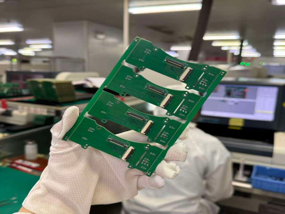
And for designs with FPC connectors, compact control sections, or mixed mechanical constraints, the same idea applies: interconnect and thermal planning can’t be separated. A flexible multilayer control PCB with FPC connector still needs copper balance, assembly discipline, and realistic heat assumptions, even if the product category looks different from a high-power BGA board.
Don’t Forget the “Non-Thermal” PCB Details
Here’s a small trap: engineers sometimes focus so hard on the heatsink that they forget the PCB fabrication choices that quietly affect assembly yield.
ENIG thickness. Solder mask dam. Pad size. Copper balance. Lamination plan. Via fill quality. Warpage. Resin recession. BGA pad flatness.
All of it matters.
A BGA package with a decent heatsink can still fail assembly if the land pattern, via-in-pad process, or PCB flatness isn’t controlled. A thermal path that looks right in CAD can become a soldering problem in SMT. And when the BGA has tight pitch, high I/O count, or mixed signal/power escape routing, thermal vias start competing with signal integrity.
This is where I’d rather review the stack-up early. Not after tooling. Not after stencil opening. Early.
Even flexible circuits have their own version of this problem. A custom flexible circuit PCB with gold pads isn’t the same as a BGA thermal board, obviously, but the lesson transfers: surface finish, copper geometry, and assembly contact quality decide whether the design behaves in real life.
Comparison Table: BGA Heatsink Interface Options
| Interface Strategy | Best Use Case | Main Advantage | Hidden Risk | My Opinion |
|---|---|---|---|---|
| Top-side heatsink on BGA lid | FPGA, processor, ASIC, AI module | Direct heat removal from package top | Poor TIM contact, uneven pressure, enclosure height limit | Strong option if the package supports it |
| BGA thermal vias to inner planes | Medium-power BGA, compact control PCB | Uses PCB copper as heat spreader | Vias do little without real copper mass | Good, but often overrated |
| Filled/capped via-in-pad | Fine-pitch BGA, HDI, dense routing | Better routing and thermal path | Higher PCB cost, tighter process control | Worth it for expensive BGA failures |
| Backside copper pad to chassis | Sealed industrial or automotive electronics | Moves heat into enclosure | Tolerance stack and insulation problems | Very good when mechanics are controlled |
| Metal-core or aluminum PCB area | LED, power module, heat-spreading sections | Short thermal path to metal base | Routing and isolation limits | Excellent for power, not universal for BGA |
| TIM gap pad to heatsink/chassis | Uneven height components | Forgives tolerance variation | Thick bond line hurts thermal performance | Useful, but often oversold |
| Airflow-only cooling | Low-to-mid power BGA | Cheap and simple | Weak in sealed or dusty enclosures | Fine only when tested |
What I’d Check Before Release
I’d ask for the uncomfortable files.
Package datasheet. Worst-case power. Ambient temperature. Enclosure model. Airflow assumption. Stack-up. Copper plane screenshots. Via structure. TIM type and thickness. Heatsink drawing. Screw torque. Chassis datum. Assembly notes. X-ray requirement. Thermal test plan.
Then I’d ask: what fails first?
The BGA solder joint? The processor junction? The nearby oscillator? A polymer capacitor? The RF section drifting? The plastic enclosure getting too warm? The user touching a hot case? The device throttling at 70°C ambient?
That question changes the design.
Because BGA thermal management is not only about keeping the chip alive. It’s about keeping the whole product believable.
FAQs
What is BGA thermal management?
BGA thermal management is the process of moving heat from a ball grid array package into the PCB, copper planes, thermal vias, TIM, heatsink, chassis, or airflow path so the chip stays below its rated junction temperature during real operating conditions. It combines PCB layout, fabrication process, assembly control, and mechanical design.
In plain shop language: don’t let the BGA become a hidden heater. The PCB has to help move heat, not just carry signals.
How do thermal vias under BGA help heat dissipation?
Thermal vias under BGA help heat dissipation by creating vertical copper paths from the BGA pad area into internal planes, backside copper, chassis contact zones, or other heat-spreading structures, reducing local hot spots when the vias are properly plated, connected, and manufactured. They work only when the destination copper is useful.
A via grid connected to weak copper is mostly decoration. Filled and capped via-in-pad is often safer for fine-pitch BGA, especially when solder wicking would damage joint quality.
What is the best PCB thermal design for BGA?
The best PCB thermal design for BGA is a verified heat-flow structure using package thermal data, copper spreading, filled or capped vias, controlled stack-up thickness, suitable TIM, reliable heatsink pressure, and real temperature testing under worst-case power and ambient conditions. No single via pattern solves every BGA design.
I don’t trust “best practice” until it survives the actual enclosure, airflow, load profile, and assembly tolerance.
Should I use a heatsink directly on a BGA package?
A heatsink should be used directly on a BGA package when the package supports top-side heat removal and the design can control TIM thickness, pressure, flatness, airflow, and mechanical loading without bending the PCB or damaging solder joints. The contact quality matters more than the heatsink catalog rating.
A big heatsink with a bad interface is just expensive metal. Sometimes the fix is not a larger heatsink, but better pressure control.
Can FR-4 handle BGA heat dissipation?
FR-4 can handle BGA heat dissipation when the BGA power level, copper area, via density, airflow, and enclosure temperature are modest enough to keep junction temperature within limits, because FR-4 itself conducts heat poorly compared with copper, aluminum, or dedicated thermal materials. The copper structure must carry most of the thermal work.
So yes, FR-4 can work. But don’t ask it to behave like aluminum.
Conclusion
Before releasing a BGA PCB, send the stack-up, BGA datasheet, estimated power dissipation, copper plane plan, via structure, TIM idea, and enclosure concept for DFM and thermal review. MC PCB can support prototype and small-batch builds where BGA thermal management, HDI routing, ENIG finish, thermal vias, and PCB heatsink interface details need to be checked before production — not after the first failure report.
