












06
Jun
Jun
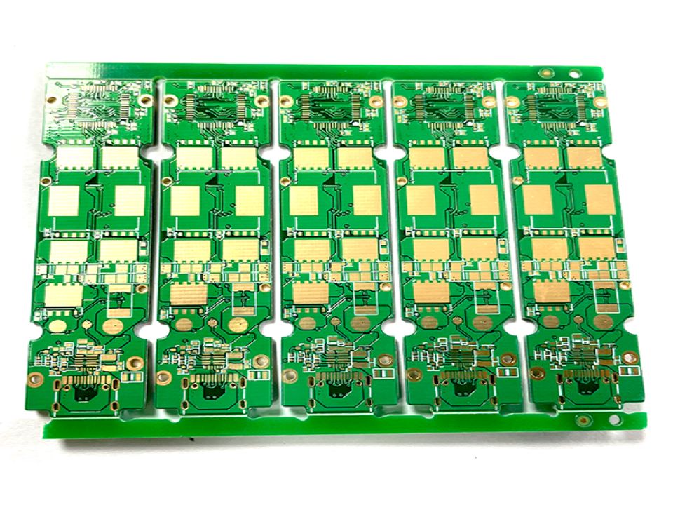
High-frequency impedance control is not only a calculator problem. It is a factory, material, copper, tolerance, and communication problem that starts with PCB stackup design.

High-frequency impedance control is not only a calculator problem. It is a factory, material, copper, tolerance, and communication problem that starts with PCB stackup design.
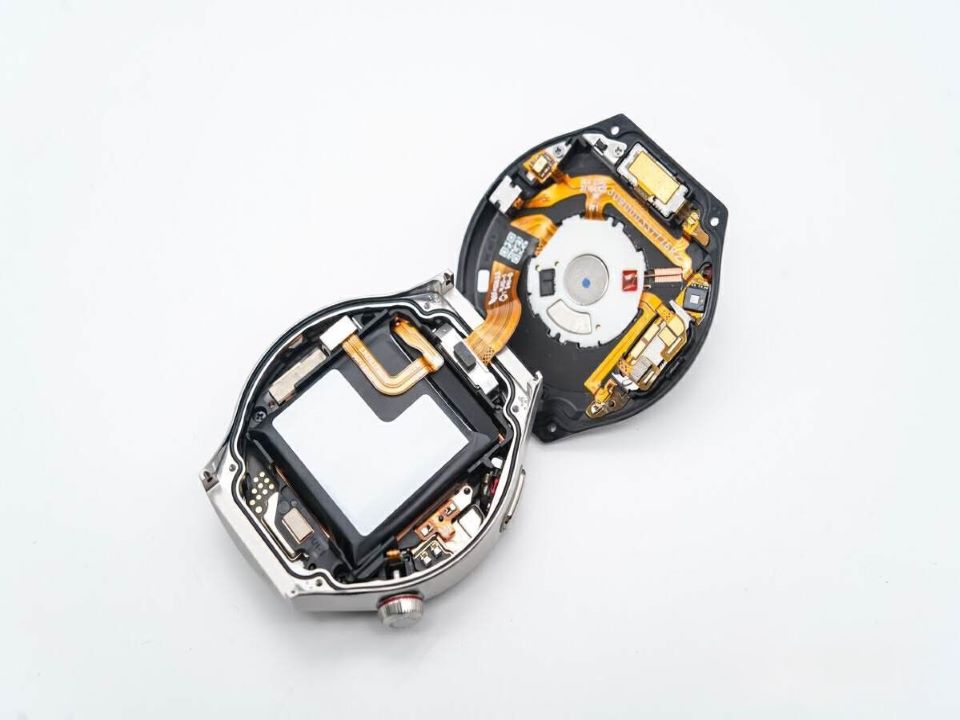
High-speed PCB design is not just faster routing; it is the discipline of keeping real electrical signals clean under imperfect materials, copper, vias, and manufacturing limits. This guide explains signal integrity fundamentals with practical layout judgment, fabrication reality, and the hard mistakes engineers usually learn too late.
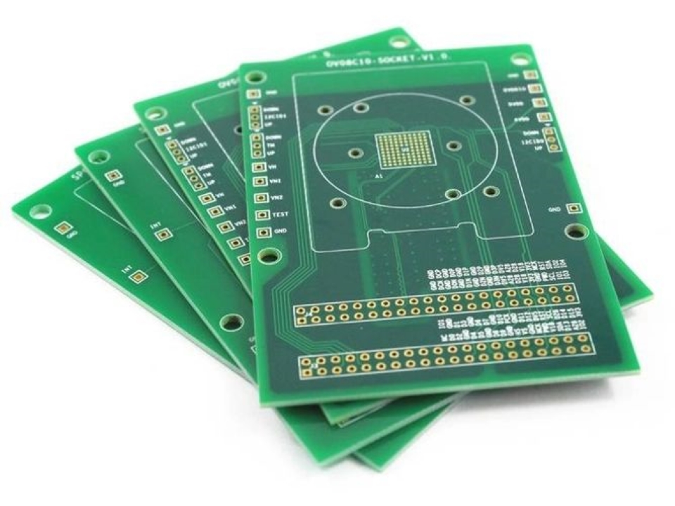
50-ohm impedance is not a magic trace width; it is a result of copper width, dielectric height, Dk, copper thickness, solder mask, and reference planes. This guide explains how PCB trace impedance calculation works before your RF or high-speed design reaches fabrication.