


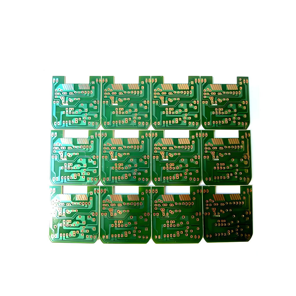
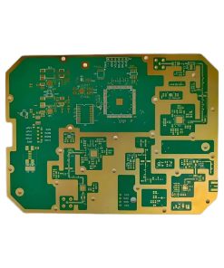
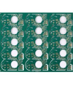
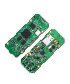
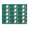
this pcb is made for signals that do not forgive shortcuts. the panel format shows multiple identical boards processed together, which improves dimensional consistency and helps keep impedance targets stable across production lots. the dense via fields and uniform pad arrays indicate a design intended for controlled routing and repeatable assembly, typical in rf front ends, antennas, power amplifiers, and wireless communication modules.
using rogers high-frequency laminates helps reduce dielectric loss and maintain predictable performance at higher frequencies, where standard fr-4 can introduce more attenuation and variation. controlled impedance traces keep reflections in check, supporting cleaner waveforms, better matching, and more reliable system-level tuning. the enig surface finish adds flat, oxidation-resistant pads that solder well and support fine-pitch components without unevenness.
for b2b oem manufacturing, delivery can include stackup engineering, impedance coupon testing, aoI inspection, and electrical test to verify continuity and isolation. the result is a multilayer rf-ready pcb that behaves consistently from prototype validation to volume production, helping your team spend less time chasing drift and more time shipping stable wireless products.
Reviews
There are no reviews yet.