


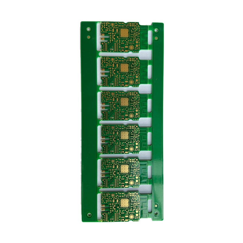
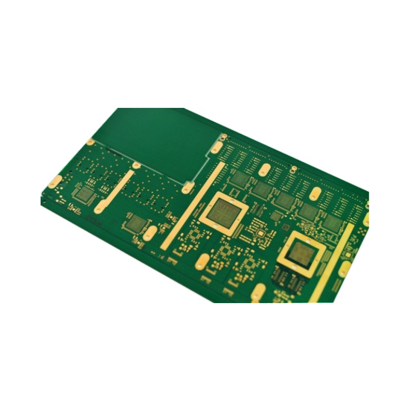
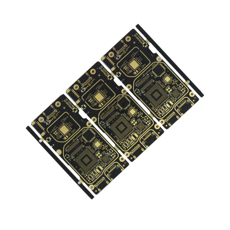
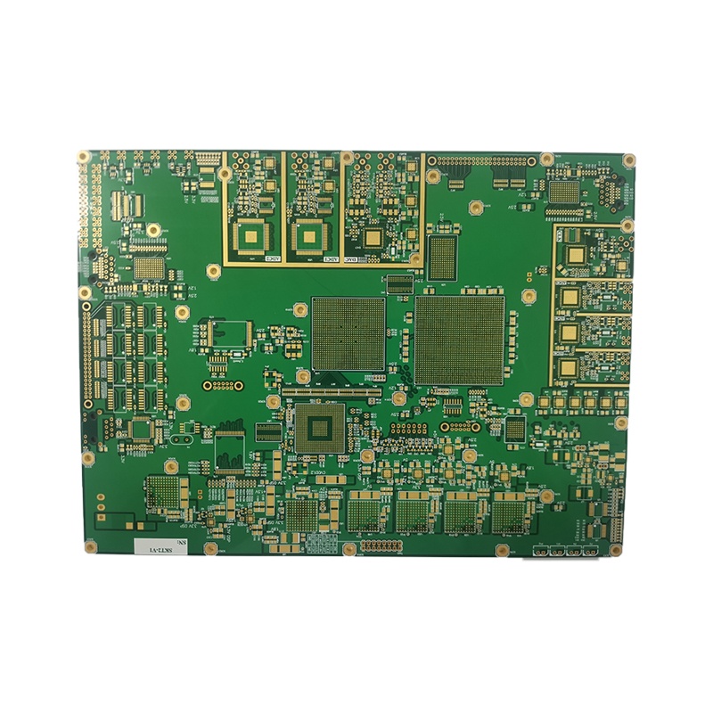
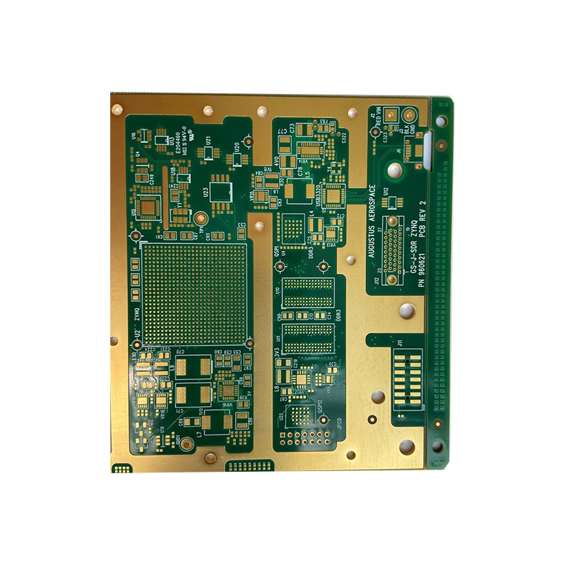
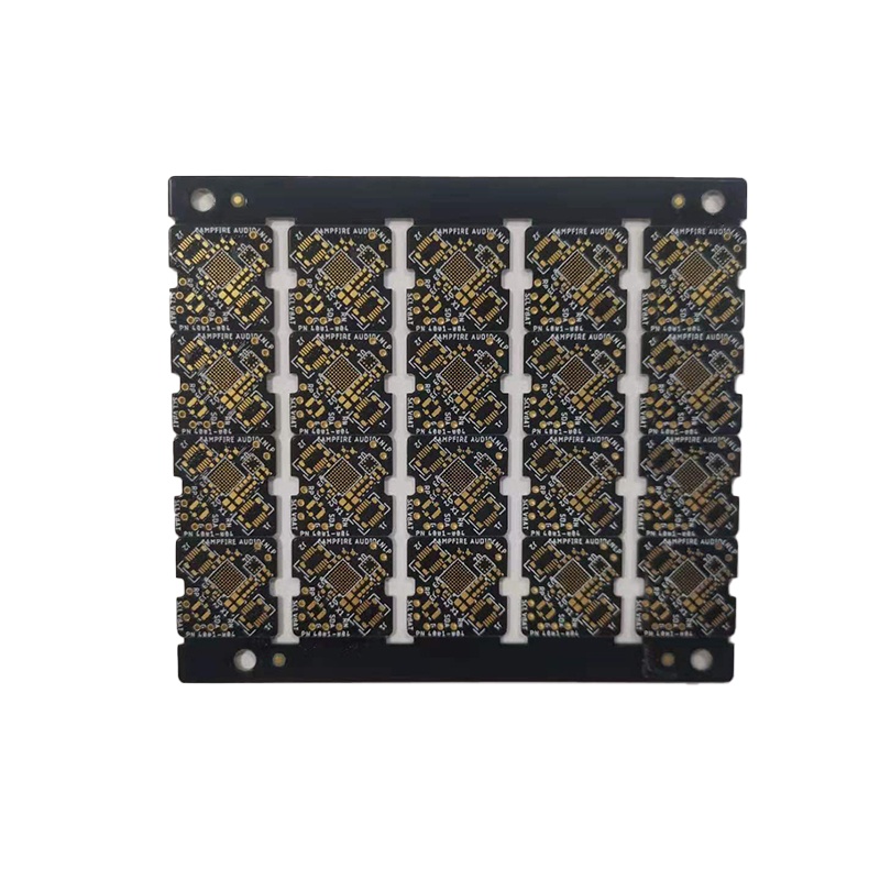
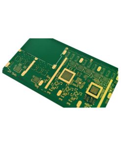
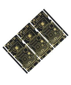
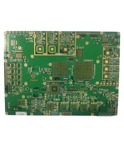
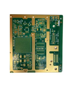
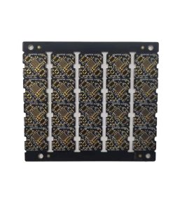
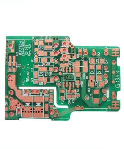
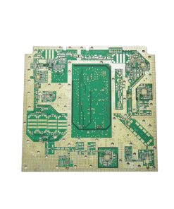
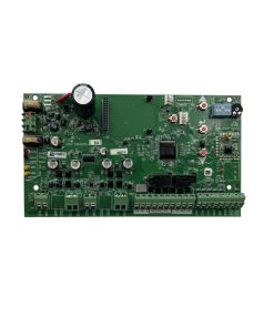
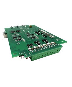
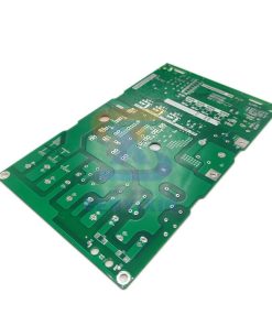
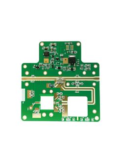
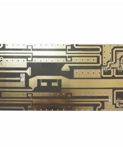
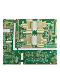
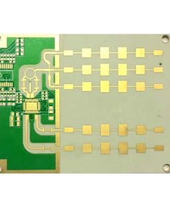
this high-precision hdi board is designed for modern rf and high-speed digital products where every millimeter of routing matters. blind and buried vias let you move signals between internal layers without opening unnecessary holes through the entire stack, which helps preserve routing space, improve impedance consistency, and reduce unwanted coupling. the gold-finished pads shown in the image support fine-pitch assembly with stable solderability, making the board suitable for bga, qfn, and other dense footprints.
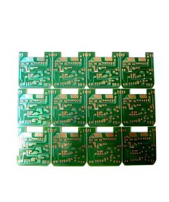
as an oem pcb supplier, we work directly from your Gerber files and provide engineering feedback to protect yield before production begins—stack-up confirmation, controlled impedance targets, via structures, and copper balancing. each build can include aoI, electrical testing, and assembly-ready panelization so the transition from prototype to volume is smooth, traceable, and repeatable for b2b programs.
Reviews
There are no reviews yet.