



















Buyer Guides
Transmission Line Loss Minimization in RF PCBs
Jul
Loss lies.
I’ve seen a board look “perfect” on screen, pass the usual impedance calculator check, use a laminate that sounded expensive enough to calm everyone in the meeting, and still come back with ugly insertion loss because the launch, copper profile, via stub, and reference return were treated like background noise. Bad move.
Why does this keep happening?
Because RF PCB Design is not a laminate-shopping exercise. It’s a pile-up of small sins: dielectric loss, conductor loss, copper roughness, impedance mismatch, solder mask loading, via transition loss, connector launch discontinuity, and sometimes—let’s be honest—wishful thinking from both design and purchasing teams.
Here’s the ugly truth: low-loss RF PCB materials won’t save a lazy RF layout.
Transmission Line Loss Is Not One Loss
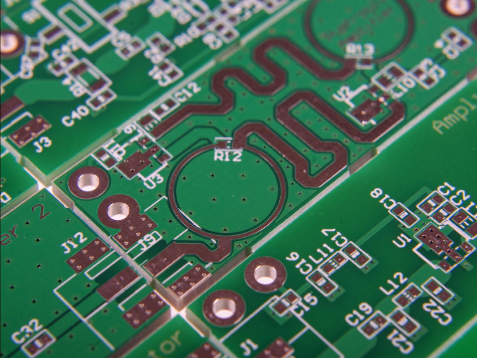
In RF PCB design, there is a concept called transmission line loss, and many people are unsure what it refers to. To put it simply, an RF signal is like a new car: as it travels along a bumpy road—such as a microstrip line, stripline, or grounded coplanar waveguide, commonly known as a controlled impedance path—its usable power is lost. This loss cannot be eliminated because it stems from dielectric absorption, skin effect resistance in the copper foil, copper foil surface roughness, via structures, radiation, impedance discontinuities, and connector transitions.
Sounds tidy.
It isn’t.
At 1 GHz, a short FR-4 feed may behave well enough. At 5.8 GHz, it starts asking questions. At 24 GHz or 77 GHz, every pad, ground void, solder mask decision, and via barrel becomes part of the RF story. No free geometry. No magic 50 ohms. No “just copy the old footprint.”
I frankly believe many RF failures begin before layout even starts. The stack-up gets treated like an admin document. Then the layout engineer is expected to fix physics with trace width.
Good luck with that.
Start With Stack-Up, Not the Trace
But everyone wants to talk about trace width first.
Wrong order.
The dielectric height, copper weight, resin content, prepreg flow, reference-plane distance, and final pressed thickness decide what the trace can be. If you change the dielectric from 0.203 mm to 0.508 mm, your 50-ohm line becomes a different animal. Wider trace. Different copper loss. Different radiation behavior. Different etch sensitivity.
Tiny change. Big headache.
On compact control products, the fight gets worse because RF routing often sits near MCU sections, LED indicators, buck converters, connectors, and noisy return currents. A product like a DC power control PCB with LED display shows the kind of mixed environment where power layout, display pads, and signal routing need discipline before anyone even says “RF.”
And if the board has wireless control, don’t let the MCU area bully the RF feed. A long-range control PCB with MCU board is exactly the sort of board where RF range can quietly lose margin through sloppy routing, weak return paths, or a bad antenna feed.
Dielectric Loss: The Quiet RF Tax
Dielectric loss is the board material eating RF energy.
The field isn’t living only inside copper. It travels through the laminate system too, which means Dk, Df, moisture behavior, resin chemistry, glass weave, and frequency stability all matter. That’s why “use low Df material” is true but still incomplete.
I’ve watched teams pay for a better laminate and then route the RF path through three unnecessary vias. Painful.
Low-loss RF PCB materials help most when the frequency is high, the RF path is long, or the design has a tight link budget. A short 2.4 GHz antenna feed may not justify a microwave laminate. A long 10 GHz stripline probably does. A radar board? Different conversation entirely.
Material names get attention. Geometry does the damage.
| Material / Structure Choice | Typical RF Behavior | Main Risk | Practical Opinion |
|---|---|---|---|
| Standard FR-4 | Acceptable for short, lower-frequency RF paths | Dk/Df variation, higher loss | Fine for cost-sensitive sub-3 GHz designs if loss budget is loose |
| High-Tg / improved FR-4 | Better process stability, still not true microwave laminate | Can still be lossy at higher GHz | Useful for mixed digital/RF boards where RF path is short |
| PTFE / ceramic-filled hydrocarbon laminates | Lower dielectric loss, better RF consistency | Cost, processing control, bonding complexity | Worth it when RF path length or frequency makes loss visible |
| Hybrid stack-up | Balances RF performance and cost | Lamination mismatch, CTE, registration | Strong option, but only if the fabricator understands mixed material builds |
| Stripline inside multilayer PCB | Better shielding, lower radiation | Higher dielectric participation, via transitions | Good for isolation, but not automatically lower loss than microstrip |
Copper Loss: Skin Effect Has No Mercy
Copper looks simple until RF shows up.
At high frequency, current rides near the copper surface. Skin effect. That means surface roughness matters more than many buyers want to hear. Rolled copper, reverse-treated copper, very-low-profile copper, and ordinary ED copper don’t behave the same once the frequency climbs.
Small hills matter.
A smooth-copper simulation can look gorgeous. The real board may not. Add plating variation, etch compensation, solder finish, and nickel under ENIG, and suddenly the conductor path is not the clean copper ribbon your field solver imagined.
Do I hate ENIG for RF? No. That’s lazy thinking. ENIG can be perfectly reasonable when solderability, shelf life, and assembly process matter. But nickel is not invisible at higher frequency, so don’t choose surface finish like it’s only a warehouse decision.
For assembled boards, this gets even messier. A dense mobile phone motherboard PCBA turnkey assembly is a good reminder: RF, digital, power, grounding, soldering, and component placement all squeeze into the same small real estate. One “minor” copper or finish decision may not stay minor.
Impedance Matching Is Not Loss Minimization
RF PCB impedance matching reduces reflected power from discontinuities, while transmission line loss minimization reduces the energy actually dissipated, absorbed, or radiated along the path. A board can show acceptable return loss and still have poor insertion loss if dielectric loss, conductor loss, via loss, or launch loss is too high.
That part gets missed constantly.
Return loss says, “How much came back?” Insertion loss says, “How much survived?” Different questions. Different pain.
So when somebody says, “The line is 50 ohms, so why is loss high?” I already know the review is going to be unpleasant. Maybe the line is too long. Maybe the copper is rough. Maybe the solder mask is loading the outer-layer microstrip. Maybe the connector launch is a tiny disaster wearing a gold finish.
It happens.
Microstrip vs Stripline: Stop Treating It Like Religion
Microstrip is easier to probe, easier to tune, and sometimes lower in dielectric loss because part of the field rides in air. Stripline is better shielded, cleaner for dense multilayer routing, and less exposed to surface contamination or solder mask weirdness.
So which is better?
Depends. Annoying, but true.
For antenna feeds and connector launches, microstrip or grounded coplanar waveguide often makes sense. For protected internal RF paths, stripline may be safer. But stripline usually needs via transitions, and those transitions can create their own loss and discontinuity.
Pick the structure after checking frequency, line length, isolation, stack-up, via count, test access, and fabrication tolerance. Not because “we always use layer 1.”
That phrase costs money.
A multilayer PCB panel with USB and Ethernet ports isn’t automatically an RF board, but it shares the same discipline: controlled impedance, return-path continuity, connector transitions, and layer-stack repeatability. RF just punishes the mistakes faster.
Connector Launches: The Usual Crime Scene
I don’t trust library RF footprints until proven otherwise.
There, I said it.
An SMA, U.FL, MMCX, board-edge RF connector, or module pad is not just a pad. It’s a transition from coaxial geometry into planar transmission line geometry. The ground via pattern, anti-pad clearance, solder volume, pad extension, reference plane shape, and trace neck-down all matter.
Generic footprint. Generic loss.
A proper launch usually needs tight ground stitching, controlled pad geometry, no random copper voids, no long signal via stub, and no surprise solder mask over the RF section unless it was part of the impedance model. If the datasheet gives a launch recommendation, start there. Then adapt it to the real stack-up, not the imaginary one.
And if the launch has never been built with that material thickness before, don’t pretend simulation equals production.
Vias Are RF Events
A via is not just a hole.
At RF, it brings inductance, capacitance, discontinuity, possible resonance, and a return-path problem if ground vias are missing. Long unused via barrels become stubs. Stubs become traps. Traps become late-night debugging.
Want to reduce transmission line loss in RF PCBs? Remove unnecessary layer changes first. Then shorten the unavoidable ones. Use blind vias or back-drilling when the stub length becomes electrically meaningful. Place return vias close enough that the return current doesn’t wander around the board like it’s lost.
And never, never cross a split reference plane with an RF trace unless you enjoy self-inflicted problems.
A mixed design like a PCB prototype with flex circuit and control board makes this point well: once rigid areas, flex tails, connectors, and control circuits share the same product, current return and transition geometry stop being “PCB details.” They become product risk.
Fabrication Tolerance: The Part Nobody Puts in the Hero Slide
Designers love clean numbers. Buyers love clean prices. Fabricators live in messy tolerance bands.
Etch width moves. Copper thickness moves. Dielectric height moves after pressing. Resin flows. Glass weave shifts local dielectric behavior. Registration isn’t perfect. Surface finish adds its own stack of consequences. Solder mask changes outer-layer impedance.
That’s normal manufacturing.
The mistake is pretending it isn’t.
A realistic RF PCB Design should be reviewed with the fabricator before final Gerber release. Not after the first failed prototype. Not after the customer asks why the range is lower. Before.
For microcontroller-heavy boards, even non-RF layout choices can create trouble if the return paths and connector areas are messy. An Atmel control PCB board with connectors is a useful example of why connector placement, control routing, and manufacturable geometry need to be considered together.
Practical Loss-Minimization Checklist
Keep this near the release checklist. Seriously.
| Design Area | What to Check | Why It Reduces Loss | Red Flag |
|---|---|---|---|
| Laminate | Dk, Df, thickness tolerance, frequency data | Reduces dielectric uncertainty | Only using generic FR-4 data |
| Copper | Copper profile, finished thickness, plating | Reduces conductor and roughness loss | Ignoring copper roughness above several GHz |
| Stack-up | Reference-plane distance, prepreg/core selection | Controls impedance and field distribution | Stack-up confirmed after layout |
| Transmission line | Microstrip, stripline, GCPW geometry | Maintains controlled impedance | Calculator result not verified by fabricator |
| Vias | Stub length, return vias, transition model | Reduces discontinuity and resonance | Long unused via barrels |
| Launches | Connector footprint, ground via fence, pad size | Reduces local mismatch | Generic library footprint |
| Solder mask | Mask over RF trace or clearance strategy | Controls outer-layer impedance shift | No rule defined |
| Surface finish | ENIG, immersion silver, OSP, hard gold | Affects solderability and RF conductor behavior | Chosen only by default purchasing habit |
| Test coupon | Impedance coupon, RF coupon if needed | Verifies actual build | No measurement plan |
| Fabricator review | Pre-build DFM and stack-up check | Catches tolerance traps | Gerber sent with no RF notes |
Cheap RF Boards Can Become Very Expensive
Cheap doesn’t always fail loudly.
Sometimes it fails as weak range. Or unstable calibration. Or random sensitivity drift. Or a second prototype round. Or an EMC margin that disappears only when the customer is waCheap doesn’t usually fail with smoke.
Honestly, that would be easier.
Most of the time, it just takes a little margin here, a little margin there. The wireless range feels weaker than the datasheet promised. Calibration moves around. One prototype looks fine. The next board is strange. Someone blames the antenna. Someone else blames the IC. Maybe they’re right. Maybe not.
From my experience, the boring suspects are often the real ones: stack-up guessed too late, copper profile never discussed, a via stub nobody wanted to model, solder mask sitting where it shouldn’t, and a connector launch copied from an old project because “it worked before.”
That sentence should make people nervous.
I’m not saying every RF PCB needs premium laminate. No. That’s expensive advice pretending to be smart advice. A short 2.4 GHz feed on a compact control board is not the same problem as a long microwave route where half a dB can start a very annoying meeting.
But the board needs a loss budget.
A real one.
Then the material and stack-up need to fit that budget. Not the buyer’s habit. Not the engineer’s favorite laminate. Not whatever was used last time.
“Just use FR-4” is lazy.
“Just use Rogers” can be lazy too.
Same shortcut. Different bill.
The question I’d rather ask is this: what’s the lowest-cost stack-up that still protects insertion loss, impedance control, repeatability, assembly yield, and test margin?
That’s the uncomfortable question. Also the useful one.
And this isn’t only an RF-board lesson. LED, display, and control boards have the same kind of hidden behavior if you stare at them long enough. Big copper pours don’t stay innocent forever. Via farms change current flow. Heat moves sideways. Return paths get chopped up by “small” layout decisions. Copper balance affects fabrication. Even a custom RGB LED PCB board assembly can remind RF designers of something basic: when the board gets small, nothing stays isolated for long.
How to Reduce Transmission Line Loss in RF PCBs
To reduce transmission line loss in RF PCBs, don’t worship the trace width. Control the whole RF path: laminate choice, pressed stack-up, copper profile, reference planes, via transitions, connector launches, solder mask rules, surface finish, and impedance verification before fabrication.
That’s the clean version.
The rough version? Stop drawing RF traces like they’re normal copper with better manners.
Every RF trace should be able to answer for itself. Why this layer? Why this width? Why this dielectric height? Why this launch? Why that via? Why that surface finish? Why is copper sitting nearby? Why is the return path broken there?
If the answer is “because the previous layout did it,” pause.
Old layouts help. They also preserve old mistakes beautifully.
A proper RF release package should include the final stack-up, target impedance, laminate type, approved substitute materials, copper weight, finished copper expectation, RF-critical net list, solder mask rule, connector launch notes, impedance tolerance, and coupon requirement.
Nobody enjoys preparing that list.
Fine.
Nobody enjoys rebuilding the same RF board twice either.
FAQ
What is transmission line loss in RF PCBs?
This brings us back to the issue of transmission line loss in RF PCBs. The specific concept was mentioned earlier, so I won’t go into it again.
On the bench, it usually shows up as insertion loss. Less insertion loss means more RF power reaches the antenna, receiver, filter, amplifier, or test point. More loss means weaker range, worse sensitivity, and less room for error. The definition is neat. The board usually isn’t.
How do low-loss RF PCB materials reduce insertion loss?
Low-loss RF PCB materials reduce contact losses through an optimized laminate system. This helps preserve the RF energy absorbed by the substrate.
But the laminate is not a magic rescue part. Rough copper still matters. Long routing still matters. Solder mask can shift things. Via stubs can waste margin. Connector launches can make a good material look mediocre very quickly.
Is microstrip or stripline better for RF PCB Design?
Microstrip is often easier to access, tune, and probe, while stripline gives better shielding and isolation inside multilayer boards. The better choice depends on frequency, routing length, radiation limits, stack-up thickness, via transitions, connector access, and production tolerance.
For antenna feeds, I’d usually expect microstrip or grounded coplanar waveguide. For protected internal RF routing, stripline may be cleaner. But there’s no automatic winner. The structure has to fit the loss budget, the enclosure, the test method, and the board house’s real process window.
Does impedance matching reduce transmission line loss?
Impedance matching reduces reflected power caused by discontinuities, but it does not remove dielectric loss, conductor loss, copper roughness loss, radiation loss, or via-transition loss. A transmission line can be well matched and still lose too much signal power along the route.
That’s where teams get tricked. Return loss tells you what bounced back. Insertion loss tells you what survived. Both numbers matter. Looking at only one is how people convince themselves the RF path is fine when it’s only fine on one graph.
How can I reduce RF PCB loss before fabrication?
You can reduce RF PCB loss before fabrication by confirming the stack-up with the PCB manufacturer, selecting suitable laminate and copper profile, shortening RF traces, avoiding unnecessary vias, cleaning up connector launches, keeping reference planes continuous, and defining solder mask and surface finish rules before Gerber release.
Early DFM review helps more than people like to admit. Once the Gerbers are frozen, the factory can still build the board, sure. But it may not be able to save an RF path based on optimistic dielectric height, rough copper assumptions, or a connector footprint that was never adapted to the real stack-up.
When should I avoid standard FR-4 for RF transmission lines?
Standard FR-4 should be avoided when frequency, line length, insertion-loss budget, phase stability, or repeatability requirements exceed what its dielectric loss and Dk variation can support. The risk becomes more obvious in higher-GHz, microwave, radar, precision measurement, and long RF-routing applications.
FR-4 isn’t evil. It’s just familiar, cheap, and too often trusted past its comfort zone. For a short RF feed, it may behave. For higher frequency, longer routing, or tight sensitivity, “FR-4 is fine” starts to sound less like confidence and more like a guess with solder mask on it.
Final Conclusion
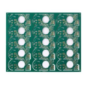
If your RF PCB is losing more power than expected, don’t blame the chip first. Send the stack-up, Gerber files, RF net notes, target impedance, material requirement, and frequency range for a DFM review. We can help check whether the real issue is laminate choice, copper profile, impedance geometry, via transitions, connector launch design, or manufacturing tolerance before the next prototype repeats the same mistake.
