













Buyer Guides
Solder Wetting on Aluminum PCBs: Process Improvements
May
Oxide wins fast.
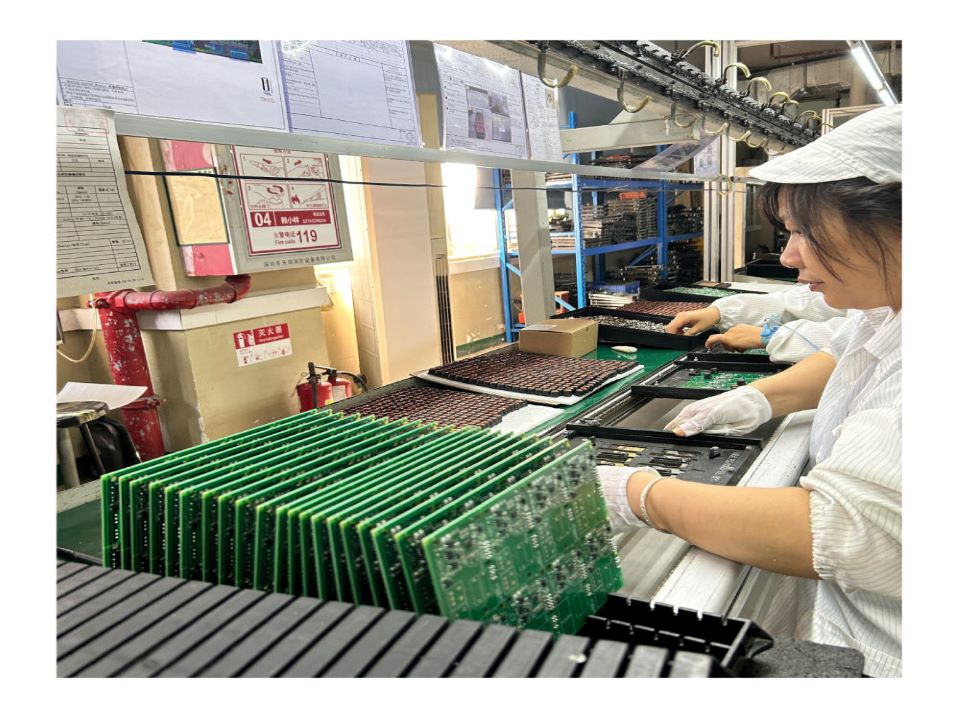
I have watched teams spend days arguing about solder paste brands while ignoring the obvious: aluminum-backed boards pull heat away from the joint, oxide contamination raises wetting resistance, and a reflow profile copied from a comfortable FR-4 job will often produce dull fillets, skipped wetting, beading, voiding, or cold-looking joints on metal-core boards. Why pretend otherwise?
The hard truth is simple: solder wetting aluminum PCBs is not mainly a solder problem. It is a surface-energy problem, a thermal-mass problem, a flux-activation problem, and sometimes a procurement problem disguised as an assembly defect.
Aluminum itself is a highly reactive metal; Britannica lists aluminum as element Al, atomic number 13, with a 660°C melting point and strong chemical activity, which matters because the native oxide behavior around aluminum-based structures is part of the reason wetting processes must be controlled aggressively.
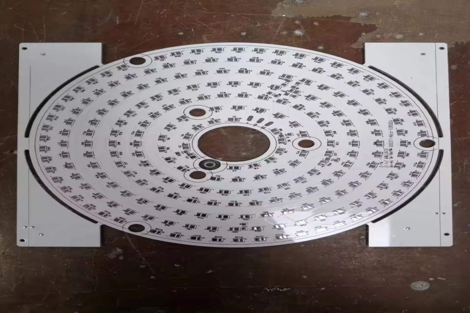
In LED lighting, power conversion, automotive lighting, grow-light modules, and compact thermal products, aluminum MCPCB is not optional anymore. The U.S. Department of Energy notes that LEDs emit little heat outward compared with incandescent and CFL lamps, yet LED products still rely heavily on internal thermal design, efficiency, and lifetime control; that is exactly why metal-core boards are common in real assemblies. For LED-heavy builds, I would rather qualify the process on a dedicated OEM LED aluminum MCPCB board than pretend a generic FR-4 solder profile tells us anything useful.
The Real Failure Mechanism: Heat Sink First, Solder Joint Second
Poor solder wetting aluminum PCB issues usually show up as one of six visible symptoms: solder balls around pads, convex beads, partial fillet coverage, dark or grainy joints, component skew, or a pad that looks “tinned” but mechanically weak.
Here is the part many factories hate hearing: the board may be innocent.
If the aluminum PCB soldering process does not deliver enough time above liquidus at the actual pad, not the oven air, not the profiler guess, not the FR-4 reference coupon, the solder never gets a fair chance. Aluminum substrate acts like a thermal sink. The copper circuit layer may be thin. The dielectric may vary. ENIG, OSP, immersion tin, or HASL each changes the wetting behavior. And on high-power LED pads, the thermal pad size can dominate the whole event.
That is why I do not trust “standard reflow.” Standard for whom?
IPC-A-610J, published March 1, 2024, is described by the Global Electronics Association as the most widely used electronics assembly acceptance standard, developed with input from 31 countries and used by inspectors and operators for assembly acceptance criteria. J-STD-001J-2024, meanwhile, is recognized globally for soldering process and material criteria and was updated with input from 27 countries.Translation for production managers: visual judgment and process control must talk to each other, or your “wetting defect” report is just theater.
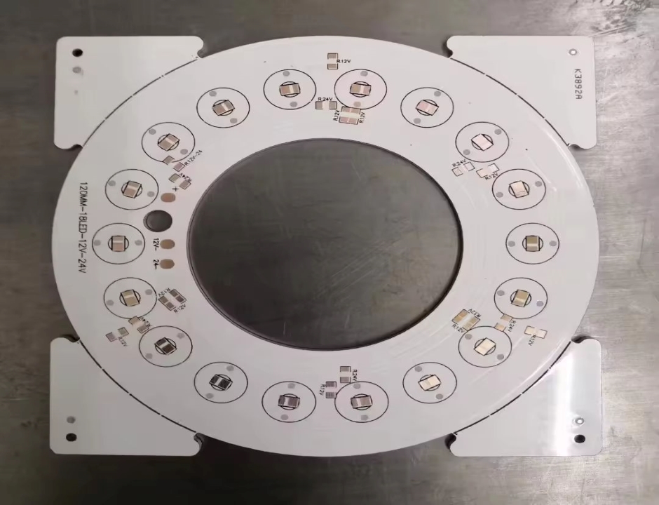
For power LED modules, the board stack matters. A double-sided MCPCB LED power supply PCB will behave differently from a simple single-sided LED strip board because copper distribution, component density, thermal vias, pad area, and aluminum base thickness all shift the heat balance.
Why Aluminum PCB Solderability Challenges Are So Persistent
The industry likes clean categories. I do not.
A defect report says “poor wetting.” The buyer says “bad PCB.” The assembler says “bad paste.” The PCB shop says “bad storage.” Everyone is partly right, which is why these fights waste money.
Improving solder wetting on aluminum circuits starts with accepting that wetting is a chain event:
| Process factor | What goes wrong | What to measure | Practical fix |
|---|---|---|---|
| Surface finish | Oxide, contamination, weak solder spread | Incoming solderability, wetting balance, visual spread | Tighten storage, packaging, finish age limits |
| Reflow profile | Pad never reaches stable wetting temperature | Thermocouple on actual pad, not nearby air | Extend soak, tune TAL, adjust ramp |
| Flux activity | Oxides not removed before liquidus | Paste spec, residue behavior, wetting spread | Match flux chemistry to finish and thermal mass |
| Stencil design | Too much or too little paste | Paste volume, aperture ratio, area ratio | Window-pane thermal pads, tune aperture reduction |
| Board thermal mass | Heat drains into aluminum base | Pad temperature delta across board | Use product-specific profiling |
| Handling | Finger oils, moisture, shop-floor contamination | Pre-bake logs, glove discipline, ionic cleanliness | Define handling rules and audit them |
| Inspection feedback | AOI catches shape, not always bond quality | Cross-section, pull/shear tests, X-ray where needed | Feed defect data back into profile and stencil design |
A 2024 Scientific Reports paper on PCB plug-in solder joint defect detection reported improved average detection accuracy from 94.45% to 96.43% using an enhanced network, which tells us something uncomfortable: inspection technology is getting better, but it still detects symptoms after the process has already failed. We should use AOI and machine vision, yes. But AOI is not a furnace engineer, not a chemist, and not a replacement for process discipline.
Process Improvement 1: Stop Copying FR-4 Reflow Profiles
FR-4 profiles are often too optimistic for aluminum PCBs.
In the real factory, I want three thermocouples minimum: one on the largest thermal pad, one on the smallest wetting-sensitive pad, and one near the coldest board edge. For dense LED boards, I prefer more. If the thermal pad hits liquidus late while small passives hit it early, you have a wetting split: some joints are cooked, some are under-wetted, and the process engineer gets blamed for “random defects.”
For SAC305, many factories target a peak around 235–245°C, but aluminum MCPCB often needs profile tuning rather than blind temperature increases. Too much peak temperature can damage LEDs, discolor solder mask, increase voiding, or stress components. Too little time above liquidus gives you incomplete wetting.
So the better question is not “what oven temperature?” It is “what pad temperature, for how long, under what flux activation window?”
For high-current designs, especially products using thick copper or ENIG finish, I would evaluate process response on a heavy copper ENIG metal core PCB before locking mass production. Heavy copper changes thermal response. ENIG changes wetting feel. Aluminum base thickness changes everything again.
Process Improvement 2: Treat Surface Finish Age Like a Yield Variable
Surface finish is not decoration. It is chemistry.
OSP ages differently from ENIG. HASL behaves differently from immersion silver. ENIG can be excellent for wetting consistency, but it can also hide problems if nickel corrosion, phosphorus imbalance, or poor storage has entered the picture. I do not like vague supplier answers like “within shelf life.” I want date code, packaging condition, humidity exposure, finish type, and whether the boards were opened, resealed, baked, or handled bare-handed.
IPC-J-STD-002E is used for solderability testing of electronic component leads, terminations, wires, lugs, and tabs, including methods and acceptance criteria for solderability and resistance to dissolution or dewetting of metallization. For bare boards, the same thinking applies: do not argue about solderability emotionally when you can test wetting behavior and separate board finish problems from assembly process problems.
A small but nasty point: baking is not magic. Excessive baking can degrade some finishes and worsen wetting. If someone says “bake everything overnight,” ask what finish, what temperature, what humidity history, and what evidence.
Process Improvement 3: Match Flux to Aluminum PCB Reality
Flux has a job: reduce oxides, protect surfaces before wetting, and allow solder to spread before it freezes.
But on aluminum PCBs, flux selection gets political. Buyers want no-clean. Quality wants low residue. Production wants aggressive wetting. Customers want cosmetics. Everyone wants miracles.
No-clean flux can work. Water-soluble flux can work. Higher-activity flux can work. The problem is mismatch. If the flux activation window closes before the large thermal pads reach liquidus, you get poor solder wetting aluminum PCB symptoms even with a decent paste. If residues remain under LEDs or high-voltage spacing, you inherit reliability risk later.
In a 2024 review of solder joint reliability under extreme conditions, researchers emphasized that temperature, mechanical stress, and radiation can affect solder microstructure, intermetallic layers, fatigue, shear strength, creep, and hardness. That is why I dislike treating wetting as cosmetic. A joint that barely wets today may become a fatigue failure after thermal cycling.
For grow lights, where high drive current and long operating hours are normal, I would connect wetting qualification directly to the end-use thermal load using a board such as an aluminum LED MCPCB panel for grow light SMD assemblies. Grow-light customers rarely forgive early field failures.
Process Improvement 4: Redesign Paste Volume Before Blaming the Operator
Bad apertures create fake chemistry problems.
On large LED thermal pads, full-open stencil apertures can trap flux volatiles and increase voiding. On small pads, excessive reduction can starve the joint. Window-pane apertures, rounded corners, area-ratio control, and local paste-volume tuning often improve wetting more than changing solder paste brand.
My rule is blunt: if the same paste wets well on a coupon but fails on the production board, look at thermal mass and aperture design before calling the paste supplier.
For mixed-technology assemblies, the contrast can be sharp. A multilayer FR4 PCB for level switch sensor cards may tolerate a different stencil philosophy than an aluminum MCPCB power board. And a flexible FPC circuit with gold fingers brings another set of surface, handling, and thermal limits. Same solder alloy does not mean same process window.
Process Improvement 5: Use Data, Not Folklore
I like operators. I do not like folklore.
“Run it hotter.”
“Use more flux.”
“Bake the boards.”
“Change paste.”
“Slow the conveyor.”
All five suggestions can be right. All five can also be expensive nonsense.
A useful aluminum PCB wetting trial should record:
| Trial item | Recommended evidence |
|---|---|
| Board finish | ENIG, OSP, HASL, immersion silver; finish date; storage condition |
| Paste | Alloy, flux class, lot number, storage temperature, thaw time |
| Stencil | Thickness, aperture design, reduction percentage, thermal pad pattern |
| Reflow | Ramp rate, soak time, peak pad temperature, TAL, cooling rate |
| Inspection | AOI images, microscope images, X-ray for voiding, cross-section if needed |
| Reliability | Shear/pull test, thermal cycling sample, powered burn-in where applicable |
| Yield | First-pass yield by defect category, not just total pass/fail |
The DOE’s 2024 final rule for general service lamps projected 4.0 quadrillion Btu of lifetime energy savings for products purchased during 2029–2058 and estimated $1.413 billion per year in net benefits, a reminder that lighting efficiency is not a boutique market but a regulated, cost-sensitive, high-volume sector. When LED products scale, soldering defects scale too. A 0.7% wetting defect rate looks small until you ship 200,000 boards.
Best-Practice Qualification Path for Aluminum PCB Wetting
Here is the sequence I would use before approving production.
First, lock the stack-up: aluminum base thickness, dielectric thermal conductivity, copper weight, solder mask, and finish. Then freeze the assembly variables: paste, stencil, reflow profile, handling, packaging, and inspection method.
Second, run a wetting DOE. Change one variable at a time: TAL, peak temperature, stencil pattern, paste type, and board precondition. Do not run a chaotic trial and call it engineering.
Third, cut boards. Cross-section the ugly joints and a few “good-looking” joints too. Pretty solder can lie.
Fourth, run stress. Thermal cycling, powered aging, or at least shear testing. The right test depends on end use, but some mechanical evidence is better than a microscope-only signoff.
Fifth, write the actual control plan. Not a generic quality statement. A real one: storage limit, humidity control, pre-bake rule, paste thaw time, stencil cleaning frequency, reflow limits, AOI defect categories, and escalation triggers.
For dense LED and power builds, I would qualify on production-like MCPCB, not a small lab coupon. A coupon tells you chemistry. A real board tells you heat.
FAQ
What causes poor solder wetting on aluminum PCBs?
Poor solder wetting on aluminum PCBs is usually caused by surface oxidation, contamination, insufficient pad temperature, weak flux activation, unsuitable surface finish age, or a reflow profile that fails to compensate for the aluminum base pulling heat away from solder joints.
The most common mistake is blaming the solder paste first. I would check pad temperature, finish condition, paste storage, stencil aperture design, and handling discipline before changing materials. Aluminum PCB solderability challenges usually come from stacked small errors, not one dramatic failure.
How do you improve solder wetting on aluminum PCBs?
You improve solder wetting on aluminum PCBs by controlling surface cleanliness, selecting a flux system matched to the board finish, profiling actual pad temperatures, increasing process evidence, and tuning stencil aperture design to balance paste volume, wetting spread, and voiding risk.
In practice, that means thermocouples on real pads, not just an oven recipe. It also means checking whether large thermal pads reach liquidus while smaller pads stay within component-safe limits. That is where many “mystery” aluminum PCB assembly techniques become measurable.
Is ENIG better for aluminum PCB soldering?
ENIG can improve soldering consistency on aluminum PCBs when the nickel-gold finish is well-controlled, fresh, and properly stored, but it is not automatically superior if nickel corrosion, poor plating control, or long storage has damaged solderability.
I like ENIG for many high-reliability MCPCB jobs because it offers flatness and storage stability. But I do not treat it as a cure-all. If the reflow profile is wrong or the flux window is mismatched, ENIG will not rescue the process.
Why does solder bead up instead of spreading on aluminum PCB pads?
Solder beads up instead of spreading when the molten solder has higher attraction to itself than to the pad surface, often because oxides, contamination, low pad temperature, expired finish, poor flux activation, or insufficient dwell time prevent proper wetting.
This is not just a visual issue. Beading can indicate weak metallurgical bonding, especially when the joint never had enough time and temperature to form a stable interface. I would verify with magnification, cross-section, or mechanical testing if the product carries meaningful load or heat.
What is the best aluminum PCB soldering process for LED boards?
The best aluminum PCB soldering process for LED boards is a controlled SMT process using verified surface finish quality, matched solder paste and flux chemistry, stencil apertures tuned for thermal pads, and a reflow profile measured directly on LED pads.
For LED boards, the solder joint is part of the thermal path. That makes wetting, voiding, and joint geometry business issues, not just assembly-room details. Poor wetting can raise thermal resistance, reduce lifetime, and create warranty pain.
Conclusion: Build the Wetting Window Before You Build the Batch
If your aluminum PCB project is fighting poor wetting, do not start by asking for “better solder.” Start with the board stack, finish, pad geometry, paste chemistry, stencil design, and real pad-temperature data.
For LED, power, automotive lighting, grow-light, and thermal-control assemblies, MCHDIPCB can support aluminum MCPCB and metal-core PCB builds with manufacturability feedback before the soldering problem reaches mass production. Ask for the board as a process system, not just a Gerber quote.
