













Buyer Guides
PCB 101: A Clear Guide to What a PCB Is in 60 Seconds
Jun
I once heard a buyer call a PCB “that green plastic thing.”
Painful sentence.
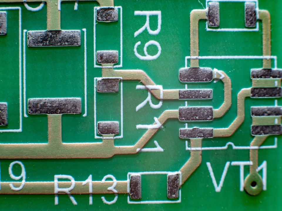
But also useful, because it shows the gap. A PCB, short for printed circuit board, is not just a green carrier for parts. It’s the controlled copper routing system that lets power, signals, heat, connectors, chips, sensors, and firmware-loaded silicon behave like one actual product instead of a fragile science project on a bench. If we were to provide a technical definition, it would be as follows: A printed circuit board provides mechanical support for circuit components and connects them electrically.
Now we come to the crux of the matter:the question that many people have: What exactly is a PCB?
A PCB is an insulating board with copper paths built into it. Components are soldered onto pads. Copper traces replace loose wires. Vias jump signals between layers. Solder mask protects exposed copper. Silkscreen gives the poor assembly guy something to read before he places the wrong connector.
That’s the polite answer.
Here’s the ugly truth: the PCB is where nice electrical theory gets dragged into laminate shrinkage, copper plating tolerance, solder wetting, impedance drift, panel utilization, warped boards, and “why is this quote higher than last time?” conversations.
It works. Usually.
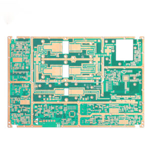
PCB Meaning: Not a Board, a Controlled Wiring System
But let’s not over-romanticize it.
A printed circuit board is basically a fixed wiring platform. The difference is that those “wires” are not loose wires anymore; they’re copper traces, copper planes, pads, and plated holes designed into a repeatable manufacturing structure. Wikipedia describes a PCB as a laminated structure with conductive and insulating layers, with components connected through copper features.
Simple? On paper.
In production, that same “simple” PCB has to survive drilling, desmear, copper plating, imaging, etching, solder mask, surface finish, routing, electrical testing, packing, shipping, SMT heat, field vibration, and maybe a customer who forgot to mention the product sits inside a hot metal enclosure.
I frankly believe this is where beginners get fooled. They learn PCB basics as vocabulary: FR-4, trace, via, pad, solder mask. Fine. Good start. But the factory doesn’t care if you know the word “via.” The factory cares whether your via aspect ratio is sane, whether your annular ring is manufacturable, and whether your 0.2 mm trace really needs to carry that current.
Not the same game.
What Is Inside a PCB?
Ever peel back a PCB mentally? Don’t imagine a flat green sheet. Think of a PCB as a thin biscuit made from fiberglass and copper.
Some PCBs have only one layer. Others are pressed together from many layers. The material may look similar, but every layer has a different copper pattern and different tiny holes called vias.
The copper patterns are like small roads. The vias are like tunnels between layers. Together, they guide power and signals through the whole electronic product.
So a PCB is not just a green board. It is a layered road system inside almost every device we use.
Inside a basic PCB, you will usually find the substrate, copper foil, solder mask, silkscreen, pads, traces, vias, and surface finish.
For a multilayer PCB, the biscuit gets more complex.
It adds inner copper layers, core materials, prepreg, reference planes, and sometimes controlled impedance structures.
Each layer has its own job. Some layers carry signals. Some help deliver power. Some provide a stable reference for high-speed circuits.
So the more advanced the PCB becomes, the more important the hidden layer structure is.That’s where the beginner-friendly picture starts getting a little dirty.
| PCB Part | What It Does | Beginner Translation | Why It Matters |
|---|---|---|---|
| Substrate | Holds the board structure | The base material | Affects strength, heat, cost |
| Copper trace | Carries current or signal | Fixed wire on the board | Width and thickness affect performance |
| Pad | Soldering area for components | Component landing spot | Bad pads cause assembly defects |
| Via | Connects layers | Copper tunnel | Needed for multilayer routing |
| Solder mask | Protects copper | Usually green coating | Reduces shorts and oxidation |
| Silkscreen | Shows text and marks | White labels | Helps assembly and repair |
| Surface finish | Protects exposed pads | Final pad coating | Affects solderability and shelf life |
Copper matters.
A lot.
You can have a gorgeous schematic and still build a bad PCB if the copper geometry is wrong. Too thin for current? Heat. Bad return path? Noise. Ugly fanout under a BGA? Re-spin. Poor copper balance? Warpage. And if nobody checks those things before production, congratulations, you’ve just bought expensive scrap with silkscreen.
For connected hardware, especially small IoT products, this becomes real fast. An OEM IoT control PCB with GSM module and SMA antennas is not only about placing a module and calling it done. Antenna clearance, ground reference, RF keep-out, connector strength, and EMI behavior all have teeth.
How Does a PCB Work?
A PCB works by replacing hand wiring with copper paths that are etched, plated, and laminated into a fixed board structure, so current and signals can move between components in a predictable way.
That sounds too clean.
In real boards, power enters through a terminal, battery pad, USB connector, pin header, FPC connector, or wire harness. Copper planes distribute current. Traces move signals. Vias connect layers. Components switch, sense, regulate, amplify, filter, communicate, and sometimes burn out because someone ignored the datasheet’s thermal note.
We’ve all seen it.
A small control board may look harmless, but add a relay, MCU, tactile switches, LEDs, and connectors, then squeeze everything into a round shape, and suddenly layout discipline matters. A round control PCB with tactile buttons and MCU has to care about button feel, copper clearance, mounting stress, and assembly repeatability. Otherwise the “basic board” becomes a customer complaint with screws in it.
And automotive? Different beast.
An OEM PoE ECU control PCB for automotive electronics can’t be treated like a toy controller. You’re dealing with temperature swings, connector reliability, vibration, current paths, protection circuits, and failure cost that makes a cheap PCB decision look very stupid later.
PCB Components: The Parts Are Only Half the Story
Ask a beginner about PCB components and they’ll usually list resistors, capacitors, ICs, sensors, and connectors.
Correct.
Incomplete.
A board also has hidden “components” in the manufacturing sense: drill holes, plated slots, copper pours, test pads, solder mask dams, fiducials, castellations, impedance traces, peelable mask sometimes, carbon ink sometimes, stiffeners on flex designs, and those tiny design choices that quietly decide whether SMT runs smoothly or your assembler starts sending angry pictures.
From my experience, component choice changes PCB cost more often than buyers expect. A BGA can force HDI. A high-current connector can force thicker copper. A fine-pitch QFN can make ENIG more sensible than cheap finish options. A GSM or RF module can demand better stack-up thinking. A big terminal block can ruin panel efficiency.
Tiny part. Big bill.
That’s why PCB basics should never stop at “what parts are on the PCB?” The better question is: what do those parts force the PCB to become?
Main PCB Types Beginners Should Know
But not every PCB is the same green rectangle.
You’ll hear single-sided, double-sided, and multilayer first. That’s the beginner layer-count language. Useful, yes. Enough? Not really.
There are rigid PCBs, flexible PCBs, rigid-flex PCBs, aluminum PCBs, HDI PCBs, high-frequency PCBs, thick-copper PCBs, high-Tg boards, ceramic boards, and mixed-material stack-ups that make quotation engineers sigh before coffee.
Each one exists because the product punishes the PCB in a different way.
LED lighting punishes heat.
Wearables punish bending.
RF products punish dielectric loss.
Industrial control punishes reliability.
Power electronics punish copper thickness.
Consumer gadgets punish cost until something fails.
For RF and microwave work, please don’t throw normal FR-4 thinking at everything. A high-frequency multilayer prototype PCB needs real stack-up control, dielectric consistency, reference planes, and impedance discipline. MCHDIPCB’s high-frequency PCB page mentions stack-up verification, impedance targets, tight etching tolerance, low-loss material options, ENIG, and 100% electrical testing.
That’s not decoration. That’s survival.
The Beginner Mistake: Treating PCB as a Commodity
Here’s the ugly truth.
A PCB can be cheap and still be wrong.
The Gerber files pass. The quote looks good. The board photo looks clean. Everyone relaxes. Then SMT starts and you see solder bridging, tombstoning, bad wetting, hole tolerance issues, weak pads, warped panels, missing test points, or a connector that technically fits but mechanically feels awful.
Nice board? No.
Just a nice-looking problem.
I’m not saying every project needs a premium PCB. That’s sales nonsense. A lot of products only need standard FR-4, 1 oz copper, normal solder mask, and a sane lead time. But you still need to know what can be standard and what must be controlled.
That’s where a B2B custom PCB prototype manufacturing service makes sense early, before volume production locks your mistakes into cartons. MCHDIPCB lists prototype-to-volume support, engineering support, QA, PCB prototype, PCB assembly, flexible PCB, rigid-flex PCB, high-frequency PCB, high-Tg PCB, thick-copper PCB, HDI PCB, aluminum PCB, and FR-4 PCB options.
The board isn’t just a purchase item.
It’s the part that makes all the other expensive parts behave.
PCB vs PCBA: Don’t Mix Them Up
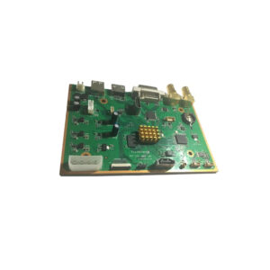
A PCB is bare.
A PCBA is assembled.
That one letter “A” matters more than people think. PCB fabrication means the board itself: laminate, copper, drilling, plating, solder mask, surface finish, routing, electrical test. PCBA means the components are mounted onto the board through SMT, through-hole assembly, reflow, wave/selective soldering if needed, AOI, X-ray for certain packages, testing, and packaging.
I’ve seen RFQs where the buyer says “PCB” but actually wants finished assembled boards. Then the supplier quotes bare PCB, the buyer compares it with a PCBA quote, and everyone wastes two days arguing over price.
Messy. Avoidable.
If your board has an SD slot, MCU, connectors, and mixed packages, you’re probably closer to a custom PCB control board assembly with SD slot than a bare PCB-only job. Send Gerber, BOM, pick-and-place, assembly drawing, test requirements, and quantity. Don’t make the factory guess.
Why PCB Cost Changes So Fast
Want the uncomfortable answer?
PCB pricing is logical, but not always intuitive.
Layer count, material type, copper weight, board thickness, surface finish, minimum trace/space, hole size, via type, impedance control, solder mask color, panel utilization, tolerance, test requirements, and lead time all push cost. Sometimes gently. Sometimes like a forklift.
A 2-layer to 4-layer change? Normal.
Through vias to blind/buried vias? Different conversation.
Standard FR-4 to low-loss RF laminate? Now we’re not playing beginner PCB anymore.
HASL to ENIG? That affects surface finish cost, storage, flatness, and fine-pitch assembly behavior.
And smaller isn’t always cheaper. I wish more product teams accepted this early. Shrinking the outline may force tighter routing, smaller vias, more layers, worse panel yield, and higher assembly pain. Cute board, ugly invoice.
So yes, what is a PCB can be answered in 60 seconds.
But making a good PCB? That takes discipline.
FAQ
What is a PCB?
What is a PCB (printed circuit board)? Think of it as the “foundation” and “highway” for electronic components. That green, rigid board you see when you take apart an electronic device (we’re just referring to the most common color here,PCBs come in many colors) is exactly what it is.
Not only does it hold all the components in place, but through the dense network of copper traces on the board, it ensures that current and signals flow precisely to where they need to go. Thanks to it, factories can use machines to automatically assemble electronic devices in bulk, eliminating the need for manual soldering of individual wires.
What does PCB stand for?
PCB stands for printed circuit board, a manufactured board made of insulating material and patterned copper that creates permanent electrical connections between electronic components such as ICs, resistors, capacitors, sensors, connectors, and power devices.
People often refer to them as “circuit boards,” but “PCB” is the more accurate term. In engineering and procurement, using “PCB” ensures that suppliers understand you are referring to a finished bare board, rather than a general electronic module or assembled product.
How does a PCB work?
A PCB uses copper traces, pads, vias, and planes to route power and electrical signals between mounted components, while the insulating substrate material keeps those conductive paths separated, supported, and stable during manufacturing and product use.
That’s the simplified explanation. The reality on the factory floor is this: every trace width, via size, copper thickness, solder mask opening, and layer transition affects whether the board assembles properly and performs reliably in the field.
What are the main PCB components?
The main components of a PCB include active components such as integrated circuits (ICs), microcontrollers (MCUs), transistors, diodes, and sensors, as well as passive components such as resistors, capacitors, inductors, fuses, and connectors. Additionally, it includes circuit board features such as traces, pads, vias, solder mask, substrate, and surface treatment.
Beginners typically calculate only the visible components. Engineers also consider the geometry of the copper foil. A missing test pad or an inappropriate via selection can have an impact on production that is just as severe as an incorrect resistance value.
What is the difference between PCB and PCBA?
A PCB refers to the bare printed circuit board before components are installed, while a PCBA refers to the assembled circuit board after components have been soldered onto it via SMT, through-hole assembly, inspection, and sometimes functional testing.
This difference significantly affects the quotation. For PCBs, suppliers require Gerber files and board specifications. For PCBAs, they also require a bill of materials (BOM), pick-and-place data, assembly drawings, testing notes, and sometimes approved component brands.
Is FR-4 always the best PCB material?
FR-4 is the most common PCB material for general electronics, but it is not always the best choice because heat, bending, high frequency, high current, tight size constraints, and reliability requirements may call for aluminum, polyimide, Rogers-type materials, high-Tg FR-4, or other substrates.
For a basic controller, FR-4 may be ideal. However, for RF applications, LED thermal boards, flexible products, power modules, or automotive electronics, choosing materials out of habit is how projects quietly become more expensive.
Conclusion
If you just need a quick answer, here it is: a PCB is the board that connects electronic components using copper traces.
But if you’re building a real product, don’t stop there.
Send the Gerber file, BOM, stack-up target, quantity, lead time, and application details before asking for the cheapest quote. A serious PCB supplier can assess manufacturability, material selection, copper thickness, surface finish, and assembly risks before the project requires a redesign.
