













Buyer Guides
PCB Testing: Standard vs Premium Options (AOI, X-ray, ICT)
May
“Can you test before shipping?”
I’ve heard this sentence too many times.
And honestly, it’s a dangerous sentence, because one factory may hear “AOI plus final visual check,” another may hear “bare-board E-test only,” while the buyer may be imagining X-ray, ICT, functional jig, test report, defect images, and a technician actually powering the thing under load.
Not the same.
PCB testing is not a sticker you put on a carton. It’s a filter. Some filters catch obvious solder bridges. Some catch buried BGA trouble. Some catch nothing useful because the board was never designed for test access in the first place.
That’s the part nobody likes.
Standard PCB Testing Isn’t Weak — Unless You Ask Too Much From It
But standard PCB testing has a job.
For a low-density FR-4 board, visible joints, no BGA, no QFN belly pad, no high-current hot spot, no RF sensitivity, no brutal field condition, standard inspection can be enough. Visual check. Bare-board open/short test. AOI PCB inspection. Final QC sampling.
Fine. Ship it.
The mistake is stretching this logic onto boards that clearly don’t belong there: 0.4 mm pitch ICs, via-in-pad, dense HDI routing, shield cans, metal-core thermal pull, weird power sequencing, and an MCU that only gets angry after firmware starts talking to the second rail.
That’s not “standard testing.” That’s gambling with nicer paperwork.
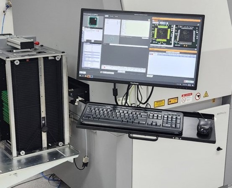
AOI PCB Inspection: Good Camera, Not a Mind Reader
I like AOI. I don’t trust it blindly.
AOI PCB inspection catches the factory classics: tombstoned resistors, missing capacitors, skewed ICs, reversed diodes, solder bridges, lifted leads, poor wetting, wrong rotation, wrong package, and the occasional feeder mistake that everyone pretends was “material variation.”
It helps. A lot.
But AOI sees surfaces. It doesn’t see under a BGA. It doesn’t know whether a QFN thermal pad has ugly voiding underneath. It doesn’t prove the net is alive. And if the golden board was rushed, or the operator keeps accepting false calls because production is already late, then AOI becomes a camera-shaped comfort blanket.
That happens.
For early-stage builds, especially a turnkey PCB assembly service for SMT PCB prototypes, AOI is still one of the first checks I’d want. Prototype issues are often physical and stupid: polarity mark confusion, footprint mismatch, paste volume trouble, rotated ICs, missing parts.
AOI catches those.
Not the buried ones.
Premium PCB Inspection Starts When the Defect Hides
What if the joint is invisible?
That’s when premium PCB inspection becomes less of an “upgrade” and more of a reality check. X-ray PCB inspection, ICT testing PCB, flying probe, functional testing, impedance checks, burn-in, coating inspection—none of these are decorative add-ons when the board has hidden failure modes.
Here’s the ugly truth: the worst defects often look polite.
A compact HDI rigid-flex PCB design with custom rigid-flex FPC may look neat on a desk, but inside that little board you can have microvias, flex-to-rigid transitions, bend stress, dense placement, connector strain, and miserable probe access.
Small board. Mean board.
And a multilayer Rogers HDI PCB mainboard for communication applications is even less forgiving. RF boards don’t care about your nice-looking solder photo if the stack-up is loose, impedance is drifting, material handling is sloppy, or the process can’t repeat across batches.
A green LED proves very little.
X-ray PCB Inspection: Pretty Boards Still Lie
I’ve seen boards that looked clean enough to photograph.
Nice alignment. Good mask. No visible bridges. Smooth solder. The kind of board that makes someone in sales relax too early.
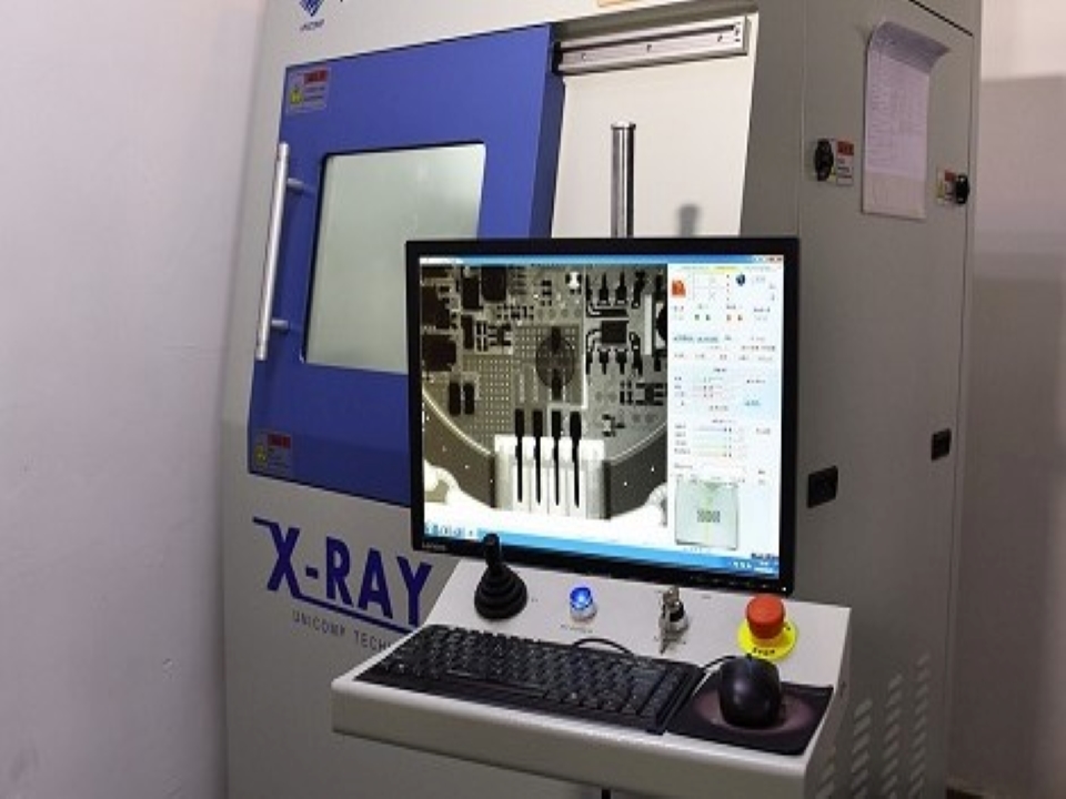
Then X-ray shows the real story: voiding under a thermal pad, suspicious BGA ball shape, hidden bridge, head-in-pillow, or a joint that’s basically waiting to become a warranty return.
Quiet disaster.
X-ray PCB inspection is for defects that hide under packages: BGA, QFN, LGA, bottom-terminated parts, dense HDI, heavy copper, large thermal pads. AOI can’t inspect what it can’t see. That sounds obvious, but it gets ignored when someone wants the quote to look cheaper.
For metal core PCB assembly for embedded smart hardware boards, I’d be especially cautious. Metal-core boards pull heat away during reflow, and that changes solder wetting, voiding, and pad behavior.
AOI says “clean.”
X-ray says “hold on.”
ICT Testing PCB: Great Tool, Terrible Afterthought
And ICT? This is where projects get messy.
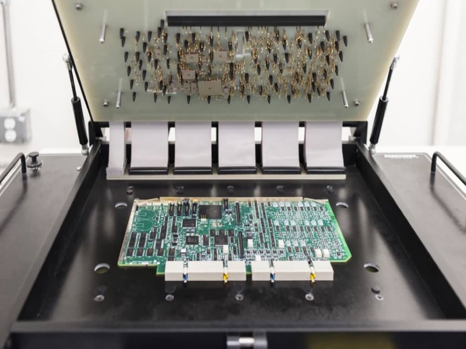
A buyer freezes the layout, approves the Gerbers, starts production planning, and then suddenly asks, “Can we add ICT?” Maybe. But where are the test pads? Can pogo pins reach the nets? Are tall components blocking access? Did anyone leave clearance? Are the rails separated enough for meaningful checks?
Often, no.
ICT testing PCB needs DFT thinking before layout lock. Test-point size, pad spacing, net access, fixture pressure, keep-outs, power sequencing, expected limits, and pass/fail rules all matter. A bed-of-nails fixture can’t probe a net that the designer buried under a chip and forgot forever.
For repeat production, though, ICT can be beautiful in a very boring way. It catches opens, shorts, wrong values, missing components, reversed parts, and a lot of assembly-level nonsense before functional test becomes a swamp.
For an IATF16949 OEM control PCB assembly manufacturer electronics program, I frankly believe test planning should start before the final layout review. Automotive-style work wants traceability, repeatability, and boring discipline.
Boring wins.
Standard vs Premium PCB Testing Options
| PCB Testing Option | Best For | What It Catches Well | What It Misses | Typical Cost Impact | My Opinion |
|---|---|---|---|---|---|
| Visual inspection | Simple boards, low-risk prototypes | Obvious solder, polarity, contamination, handling damage | Hidden joints, electrical faults, marginal solder | Low | Necessary, but weak alone |
| AOI PCB inspection | SMT boards with visible joints | Missing parts, skew, tombstones, bridges, polarity, solder defects | BGA/QFN hidden defects, electrical function | Low to medium | Best standard inspection tool |
| X-ray PCB inspection | BGA, QFN, HDI, dense assemblies | Hidden solder bridges, voids, head-in-pillow, internal joint defects | Full electrical behavior, firmware issues | Medium to high | Non-negotiable for hidden joints |
| ICT testing PCB | Repeat production, high-reliability PCBA | Opens, shorts, wrong values, component-level faults | Mechanical defects, some functional edge cases | High fixture cost, lower unit risk | Worth it when volume repeats |
| Flying probe | Prototypes, low-volume builds | Opens, shorts, basic electrical checks without fixture | High-speed functional behavior, some component faults | Medium | Good before committing to ICT fixture |
| Functional test | Finished assemblies | Real operating behavior, firmware, connectors, load response | Root cause unless paired with other tests | Medium to high | The closest test to customer reality |
How to Choose PCB Testing Options Without Wasting Money
Don’t buy tests like toppings on a pizza.
More is not automatically smarter.
From my experience, the right question is blunt: what can fail, where can it hide, and will this test actually catch it? If the defect is visible, AOI may be enough. If it sits under a package, use X-ray. If it’s electrical but not fully functional, flying probe or ICT makes sense. If the board must behave like the final product, build a functional test.
Simple idea. Hard conversation.
A custom multilayer PCB and PCB assembly OEM supplier service shouldn’t quote “testing” as one vague line. The quote should separate bare-board electrical test, SMT AOI, X-ray sampling or 100% X-ray, flying probe, ICT, functional test, and outgoing QC.
Otherwise, “tested” means almost anything.
Which means nothing.
Premium Testing Still Can’t Fix Bad Front-End Decisions
However, premium inspection won’t save a bad design.
Bad footprints, missing polarity marks, unclear BOM alternates, no test pads, terrible probe access, weak stencil aperture design, uncontrolled impedance notes, mystery substitutions, and last-minute Gerber changes all create problems that inspection can only discover later.
Testing finds the wound.
It doesn’t stop the knife.
For flexible FPC circuit board assembly for custom FPC cables, solder isn’t the only thing that matters. Bend radius, stiffener position, coverlay window accuracy, connector fit, pad cracking, handling marks, and assembly stress can all wreck a part that passed electrical test five minutes earlier.
That’s FPC life.
Send the dull files early: Gerber, BOM, centroid, assembly drawing, IPC class target, coating zones, firmware notes, connector notes, test spec, and old failure photos if they exist. Nobody loves paperwork. But missing information makes factories guess.
Guessing ships defects.
When Standard PCB Testing Is Enough
Standard PCB testing is enough when the board is simple, visible, stable, and low-risk.
Basic controller? Fine.
Simple LED board? Often.
First prototype for fit and SMT validation? Sure, AOI plus basic inspection may be enough.
But once the board includes BGA, QFN, hidden pads, HDI routing, high current, RF sensitivity, thermal stress, FPC bending, automotive expectations, or expensive downstream rework, stop pretending standard inspection is “basically the same.” It isn’t.
That’s budget pressure talking.
When Premium PCB Inspection Is Worth It
Premium PCB inspection is worth it when failure is hidden, expensive, intermittent, safety-related, or painful to debug after shipment.
Use X-ray for BGA, QFN, LGA, bottom-terminated packages, dense HDI, metal-core thermal behavior, and suspicious reflow windows. Use flying probe for low-volume builds where an ICT fixture doesn’t make sense. Use ICT when the volume repeats and the PCB has test access. Use functional testing when real operation matters.
Power rails. Firmware. Sensors. Relays. Loads. Connectors. Communication ports.
That’s where boards stop pretending.
FAQ
What is PCB testing?
PCB testing is the process of checking a bare PCB or assembled PCBA for electrical faults, soldering defects, assembly errors, mechanical issues, and functional performance before shipment, using methods such as AOI, X-ray inspection, flying probe, ICT, visual inspection, and functional testing.
In factory language, it’s the difference between “made” and “verified.” A bare board may only need open/short testing. A dense PCBA with BGA or QFN packages may need AOI, X-ray, and functional testing before anyone should trust it.
What is the difference between standard PCB testing and premium PCB inspection?
Standard PCB testing usually covers baseline inspection methods such as visual checks, bare-board electrical testing, and AOI for visible SMT defects, while premium PCB inspection adds deeper methods like X-ray, ICT, flying probe, functional testing, and custom reporting for higher-risk assemblies.
The real difference is detection depth. Standard testing catches obvious process defects. Premium inspection targets hidden solder issues, electrical faults, repeatability problems, and failures that may only show up after power, heat, vibration, flexing, or customer use.
Is AOI enough for PCB assembly testing?
AOI is enough for many simple PCB assemblies with visible solder joints, low component density, stable SMT placement, and limited field-failure risk, but it is not enough for hidden joints, BGA packages, QFNs, high-density layouts, or safety-critical applications.
AOI is a gate, not a guarantee. It’s strong at catching tombstones, bridges, missing parts, skew, polarity issues, and ugly solder. It’s weak when the problem sits under the component or only appears electrically.
When should I use X-ray PCB inspection?
X-ray PCB inspection should be used when the PCBA contains hidden solder joints, BGA, QFN, LGA, bottom-terminated packages, dense HDI layouts, high-reliability requirements, or thermal conditions where optical inspection cannot confirm solder quality.
Use it during first-article builds, NPI, BGA-heavy assembly, metal-core production, and any project where a hidden solder defect would be expensive to chase later. AOI can’t inspect what it can’t see. That’s the whole point.
Is ICT testing worth the cost?
ICT testing is worth the cost when the PCB assembly has repeat production volume, proper test-point access, high reliability requirements, and enough electrical complexity that catching opens, shorts, wrong values, and component faults early will reduce rework and field failures.
For five prototypes, ICT often feels excessive. For thousands of repeat units, it can save real money. The catch is boring but serious: ICT must be designed into the PCB before layout lock.
How do I choose PCB testing options for my project?
Choose PCB testing options by matching each test method to the board’s real failure risk: AOI for visible SMT defects, X-ray for hidden solder joints, flying probe for low-volume electrical checks, ICT for repeat production, and functional testing for final operating behavior.
Don’t choose by habit. Choose by package type, production volume, test access, field-failure cost, operating stress, and rework difficulty. The board usually tells you what testing it needs—if you’re willing to listen.
Conclusion
If your board has BGA, HDI routing, FPC sections, high-current copper, RF materials, thermal stress, or automotive-style reliability pressure, don’t ask for “PCB testing” as one vague checkbox. Send the Gerber, BOM, assembly drawing, target application, and known risk points. We’ll help you choose standard or premium inspection based on the board’s real failure modes—not just a nice-looking QC label.
